|
|
|
|
|
|
|
|
|
|
|
|
|
| CY14B256K | |
|
|
|
|
|
|
|
|
|
|
|
|
|
|
| |
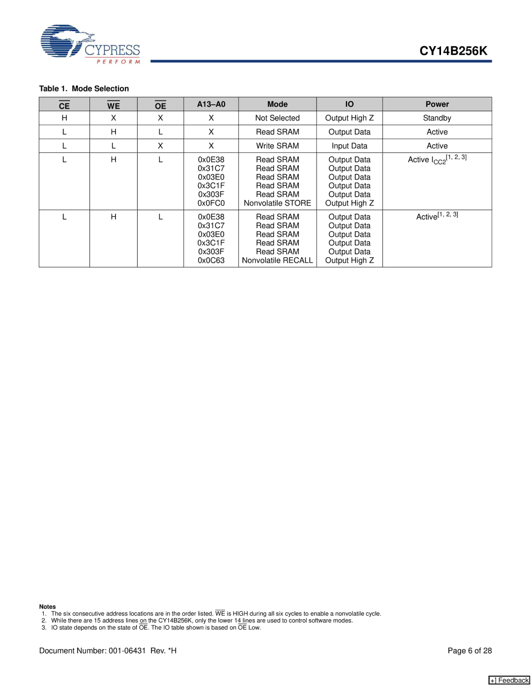
Table 1. Mode Selection |
|
|
|
|
|
|
|
|
| ||||||
|
|
|
|
|
|
|
|
|
|
|
|
|
|
| |
|
|
|
|
|
|
|
|
|
|
|
| Mode | IO | Power | |
| CE | WE |
| OE | |||||||||||
| H |
|
| X |
|
|
| X |
| X | Not Selected | Output High Z | Standby | ||
|
|
|
|
|
|
|
|
|
|
|
|
|
| ||
| L |
|
| H |
|
|
| L |
| X | Read SRAM | Output Data | Active | ||
|
|
|
|
|
|
|
|
|
|
|
|
|
| ||
| L |
|
| L |
|
|
| X |
| X | Write SRAM | Input Data | Active | ||
|
|
|
|
|
|
|
|
|
|
|
|
|
| ||
| L |
|
| H |
|
|
| L |
| 0x0E38 | Read SRAM | Output Data | Active ICC2[1, 2, 3] | ||
|
|
|
|
|
|
|
|
|
|
| 0x31C7 | Read SRAM | Output Data |
|
|
|
|
|
|
|
|
|
|
|
|
| 0x03E0 | Read SRAM | Output Data |
|
|
|
|
|
|
|
|
|
|
|
|
| 0x3C1F | Read SRAM | Output Data |
|
|
|
|
|
|
|
|
|
|
|
|
| 0x303F | Read SRAM | Output Data |
|
|
|
|
|
|
|
|
|
|
|
|
| 0x0FC0 | Nonvolatile STORE | Output High Z |
|
|
| L |
|
| H |
|
|
| L |
| 0x0E38 | Read SRAM | Output Data | Active[1, 2, 3] | ||
|
|
|
|
|
|
|
|
|
|
| 0x31C7 | Read SRAM | Output Data |
|
|
|
|
|
|
|
|
|
|
|
|
| 0x03E0 | Read SRAM | Output Data |
|
|
|
|
|
|
|
|
|
|
|
|
| 0x3C1F | Read SRAM | Output Data |
|
|
|
|
|
|
|
|
|
|
|
|
| 0x303F | Read SRAM | Output Data |
|
|
|
|
|
|
|
|
|
|
|
|
| 0x0C63 | Nonvolatile RECALL | Output High Z |
|
|
Notes
1.The six consecutive address locations are in the order listed. WE is HIGH during all six cycles to enable a nonvolatile cycle.
2.While there are 15 address lines on the CY14B256K, only the lower 14 lines are used to control software modes.
3.IO state depends on the state of OE. The IO table shown is based on OE Low.
Document Number: | Page 6 of 28 |
[+] Feedback