|
| ADVANCE | CY14E102L, CY14E102N | |
|
|
|
|
|
|
|
|
|
|
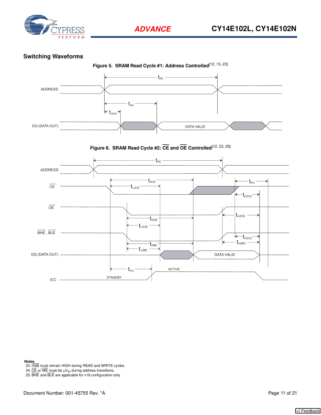
Switching Waveforms
Figure 5. SRAM Read Cycle #1: Address Controlled[12, 13, 23]
ADDRESS
tRC
tAA
tOHA
DQ (DATA OUT)
DATA VALID
Figure 6. SRAM Read Cycle #2: CE and OE Controlled[12, 23, 25]
ADDRESS
CE
OE
BHE , BLE
DQ (DATA OUT)
ICC
tRC
tACE
tLZCE
tDOE
tLZOE
tDBE
tLZBE
tPU ![]() ACTIVE
ACTIVE
STANDBY
tPD
tHZCE
tHZOE
tHZCE tHZBE
DATA VALID
Notes
23.HSB must remain HIGH during READ and WRITE cycles.
24.CE or WE must be >VIH during address transitions.
25.BHE and BLE are applicable for x16 configuration only.
Document Number: | Page 11 of 21 |
[+] Feedback