|
| ADVANCE | CY14E102L, CY14E102N | |
|
|
|
|
|
|
|
|
|
|
Pinouts (continued)
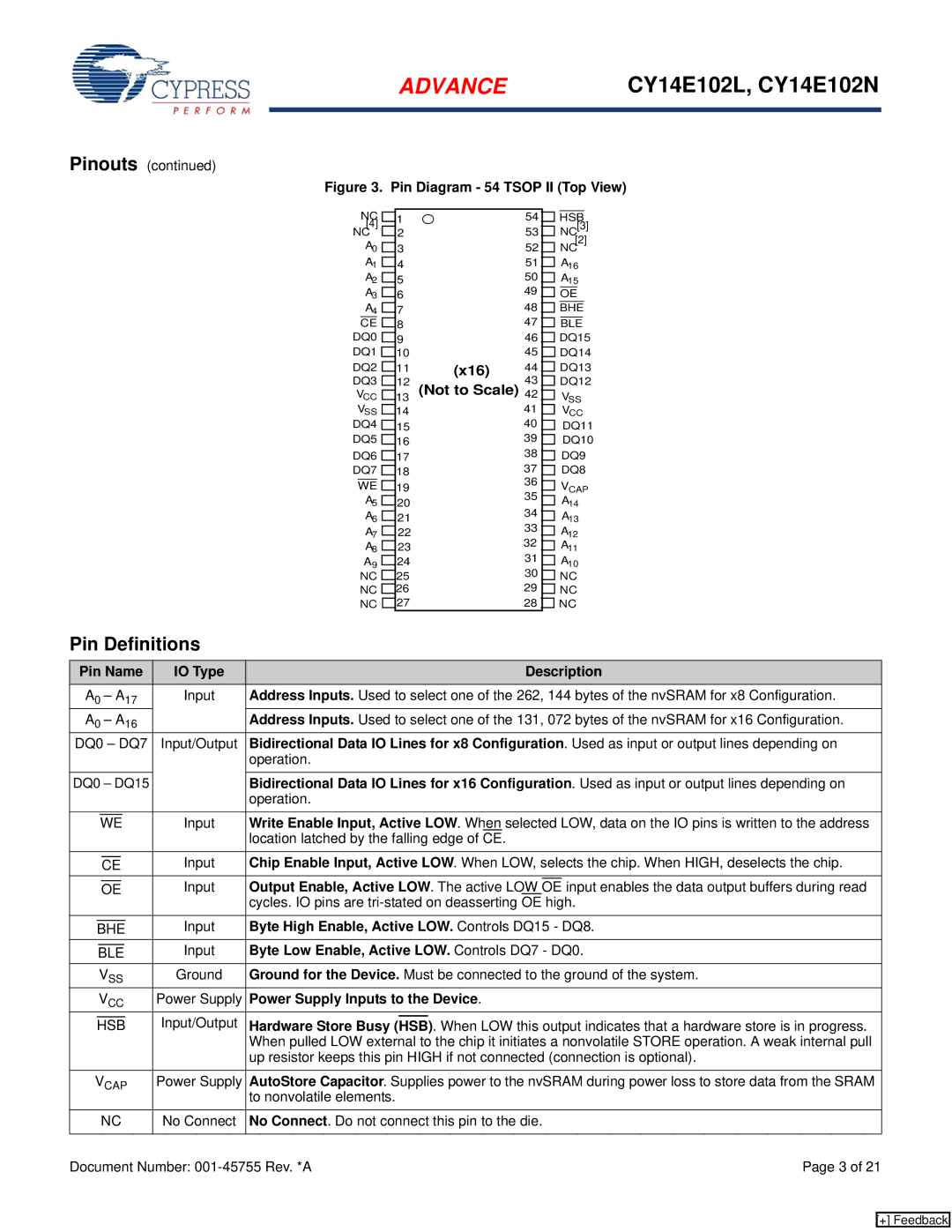
Figure 3. Pin Diagram - 54 TSOP II (Top View)
|
| NC |
|
| 1 | |||
[4] |
|
|
|
| ||||
NC |
|
| 2 | |||||
|
| |||||||
|
| A0 |
|
| 3 | |||
| ||||||||
|
| |||||||
|
| A1 |
|
| 4 | |||
|
| |||||||
|
| |||||||
|
| A2 |
|
| 5 | |||
|
| |||||||
|
| |||||||
|
| A3 |
|
| 6 | |||
|
| |||||||
|
| |||||||
|
| A4 |
|
| 7 | |||
|
| |||||||
|
| CE |
|
|
| 8 | ||
|
| |||||||
DQ0 |
|
| 9 | |||||
|
| |||||||
DQ1 |
|
|
|
| 10 | |||
|
|
|
| |||||
DQ2 |
|
| 11 | |||||
| ||||||||
DQ3 |
|
| 12 | |||||
|
| |||||||
VCC |
|
| 13 | |||||
|
| |||||||
|
| |||||||
VSS |
|
| 14 | |||||
|
| |||||||
DQ4 |
|
|
| 15 | ||||
|
|
| ||||||
|
|
| ||||||
DQ5 |
|
|
| 16 | ||||
|
|
| ||||||
|
|
| ||||||
DQ6 |
|
|
| 17 | ||||
|
|
| ||||||
DQ7 |
|
|
| 18 | ||||
|
|
| ||||||
|
|
|
|
|
|
|
| |
| WE |
|
|
| 19 | |||
|
|
| ||||||
|
| A5 |
|
|
| 20 | ||
|
|
| ||||||
|
|
| ||||||
|
| A6 |
|
| 21 | |||
|
| |||||||
|
| A7 |
|
| 22 | |||
|
| |||||||
|
| A8 |
|
| 23 | |||
|
| |||||||
|
| A9 |
|
|
| 24 | ||
|
|
| ||||||
| NC |
|
|
| 25 | |||
| NC |
|
|
| 26 | |||
|
|
|
| |||||
| NC |
|
| 27 | ||||
|
|
| ||||||
|
|
|
|
|
|
|
|
|
(x16) (Not to Scale)
54HSB
53![]() NC[3]
NC[3]
52![]() NC[2]
NC[2]
51 ![]() A16
A16
50 ![]() A15
A15
49 ![]() OE
OE
48 ![]() BHE
BHE
47 ![]() BLE
BLE
46 ![]() DQ15
DQ15
45 ![]() DQ14
DQ14
44 ![]() DQ13
DQ13
43 ![]() DQ12
DQ12
42 ![]() VSS
VSS
41 ![]() VCC
VCC
40 ![]() DQ11
DQ11
39 ![]() DQ10
DQ10
38 ![]() DQ9
DQ9
37 ![]() DQ8
DQ8
36 VCAP
35 ![]() A14
A14
34 ![]() A13
A13
33 ![]() A12
A12
32 ![]() A11
A11
31 ![]() A10
A10
30 ![]() NC
NC
29 ![]() NC
NC
28 ![]() NC
NC
Pin Definitions
Pin Name | IO Type |
|
| Description |
| |||||||||
A0 – A17 | Input | Address Inputs. Used to select one of the 262, 144 bytes of the nvSRAM for x8 Configuration. | ||||||||||||
A0 – A16 |
| Address Inputs. Used to select one of the 131, 072 bytes of the nvSRAM for x16 Configuration. | ||||||||||||
DQ0 – DQ7 | Input/Output | Bidirectional Data IO Lines for x8 Configuration. Used as input or output lines depending on | ||||||||||||
|
|
|
|
|
|
|
|
| operation. |
| ||||
|
|
| ||||||||||||
DQ0 – DQ15 |
| Bidirectional Data IO Lines for x16 Configuration. Used as input or output lines depending on | ||||||||||||
|
|
|
|
|
|
|
|
| operation. |
| ||||
|
|
|
|
|
|
|
|
|
| |||||
|
|
|
|
|
|
|
| Input | Write Enable Input, Active LOW. When selected LOW, data on the IO pins is written to the address | |||||
|
| WE | ||||||||||||
|
|
|
|
|
|
|
|
| location latched by the falling edge of CE. |
| ||||
|
|
|
|
|
|
|
|
| ||||||
|
|
|
|
|
|
| Input | Chip Enable Input, Active LOW. When LOW, selects the chip. When HIGH, deselects the chip. | ||||||
|
| CE | ||||||||||||
|
|
|
|
|
|
|
| Input | Output Enable, Active LOW. The active LOW |
| input enables the data output buffers during read | |||
|
|
|
|
|
|
| OE | |||||||
|
| OE | ||||||||||||
|
|
|
|
|
|
|
|
| cycles. IO pins are |
| ||||
|
|
|
|
|
|
|
| Input | Byte High Enable, Active LOW. Controls DQ15 - DQ8. |
| ||||
| BHE |
| ||||||||||||
|
|
|
|
|
|
| Input | Byte Low Enable, Active LOW. Controls DQ7 - DQ0. |
| |||||
| BLE |
| ||||||||||||
| VSS | Ground | Ground for the Device. Must be connected to the ground of the system. |
| ||||||||||
| VCC | Power Supply | Power Supply Inputs to the Device. |
| ||||||||||
|
|
|
|
|
|
|
| Input/Output | Hardware Store Busy |
| . When LOW this output indicates that a hardware store is in progress. | |||
| HSB |
| (HSB) | |||||||||||
|
|
|
|
|
|
|
|
| When pulled LOW external to the chip it initiates a nonvolatile STORE operation. A weak internal pull | |||||
|
|
|
|
|
|
|
|
| up resistor keeps this pin HIGH if not connected (connection is optional). |
| ||||
|
|
| ||||||||||||
VCAP | Power Supply | AutoStore Capacitor. Supplies power to the nvSRAM during power loss to store data from the SRAM | ||||||||||||
|
|
|
|
|
|
|
|
| to nonvolatile elements. |
| ||||
|
| NC | No Connect | No Connect. Do not connect this pin to the die. |
| |||||||||
|
|
|
| |||||||||||
Document Number: | Page 3 of 21 | |||||||||||||
[+] Feedback