|
| ADVANCE | CY14E102L, CY14E102N | |
|
|
|
|
|
|
|
|
|
|
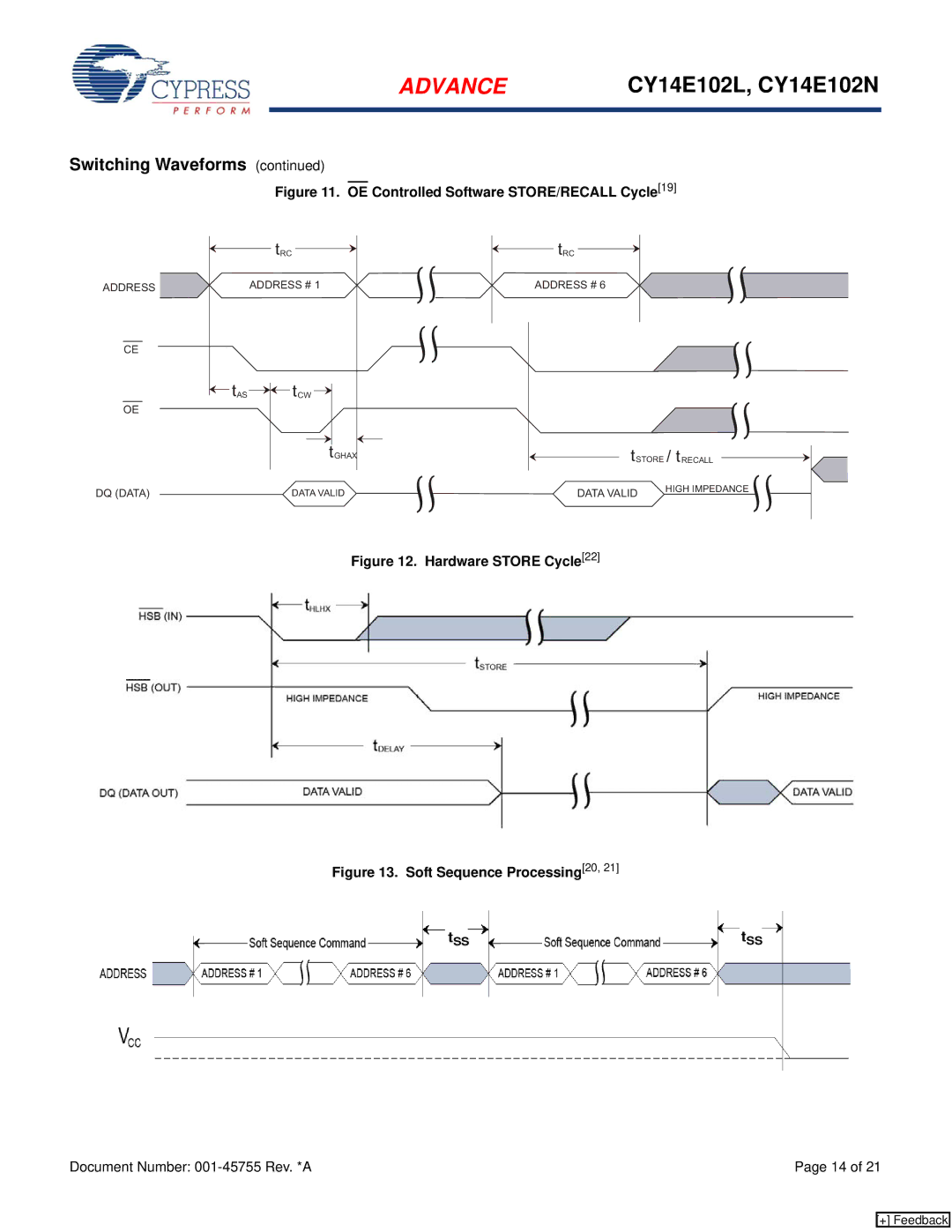
Switching Waveforms (continued)
Figure 11. OE Controlled Software STORE/RECALL Cycle[19]
ADDRESS ![]()
CE
OE
tRC
ADDRESS # 1
![]() tAS
tAS ![]()
![]() tCW
tCW ![]()
tGHAX
α α α α
tRC
ADDRESS # 6
α α α α α α
tSTORE / tRECALL
DQ (DATA) | DATA VALID |
α α
| α α |
DATA VALID | HIGH IMPEDANCE |
|
Figure 12. Hardware STORE Cycle[22]
Figure 13. Soft Sequence Processing[20, 21]
tSS | tSS |
Document Number: | Page 14 of 21 |
[+] Feedback