|
|
|
|
| ADVANCE |
| CY14E102L, CY14E102N | |||||||
|
|
|
|
|
|
|
|
|
|
|
|
|
| |
|
|
|
|
|
|
|
|
|
|
|
|
| ||
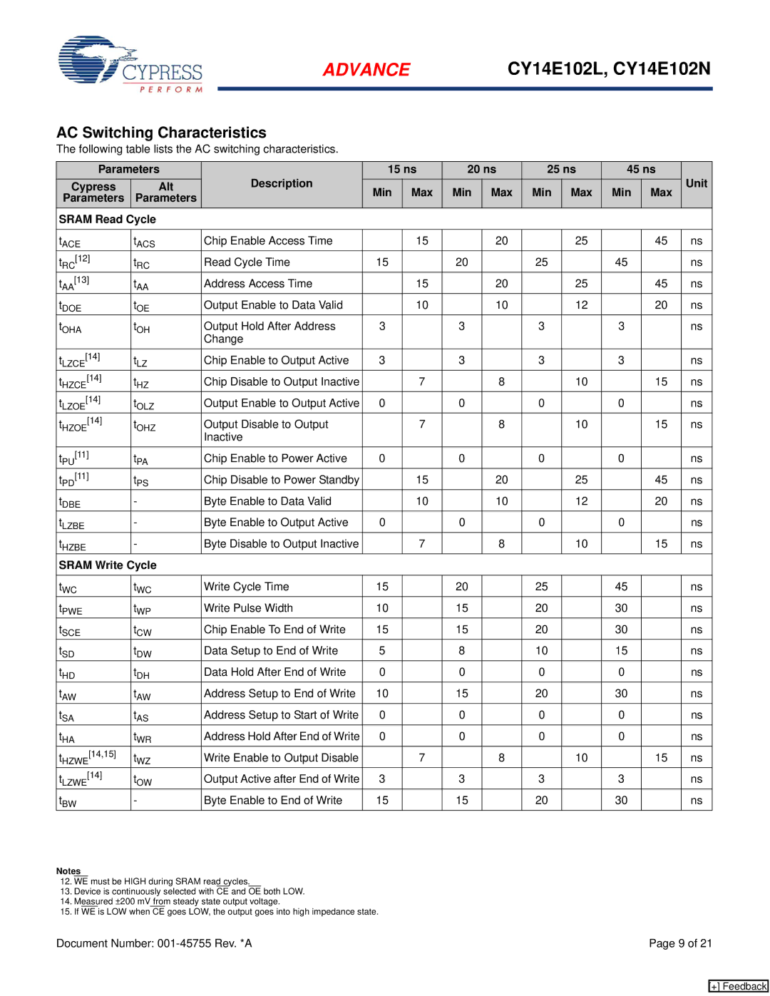
AC Switching Characteristics |
|
|
|
|
|
|
|
|
| |||||
The following table lists the AC switching characteristics. |
|
|
|
|
|
|
|
|
| |||||
|
|
|
|
|
|
|
|
|
|
|
|
|
|
|
| Parameters |
|
| Description | 15 ns | 20 ns | 25 ns | 45 ns | Unit | |||||
| Cypress | Alt |
|
| Min | Max | Min | Max | Min | Max | Min | Max | ||
| Parameters | Parameters |
|
|
|
| ||||||||
|
|
|
|
|
|
|
|
|
|
|
|
| ||
SRAM Read Cycle |
|
|
|
|
|
|
|
|
|
|
|
| ||
|
|
|
|
|
|
|
|
|
|
|
| |||
tACE | tACS | Chip Enable Access Time |
| 15 |
| 20 |
| 25 |
| 45 | ns | |||
tRC[12] | tRC | Read Cycle Time | 15 |
| 20 |
| 25 |
| 45 |
| ns | |||
t | [13] | t | Address Access Time |
| 15 |
| 20 |
| 25 |
| 45 | ns | ||
| AA | AA |
|
|
|
|
|
|
|
|
|
|
|
|
tDOE | tOE | Output Enable to Data Valid |
| 10 |
| 10 |
| 12 |
| 20 | ns | |||
tOHA | tOH | Output Hold After Address | 3 |
| 3 |
| 3 |
| 3 |
| ns | |||
|
|
| Change |
|
|
|
|
|
|
|
|
| ||
tLZCE[14] | tLZ | Chip Enable to Output Active | 3 |
| 3 |
| 3 |
| 3 |
| ns | |||
tHZCE[14] | tHZ | Chip Disable to Output Inactive |
| 7 |
| 8 |
| 10 |
| 15 | ns | |||
tLZOE[14] | tOLZ | Output Enable to Output Active | 0 |
| 0 |
| 0 |
| 0 |
| ns | |||
tHZOE[14] | tOHZ | Output Disable to Output |
| 7 |
| 8 |
| 10 |
| 15 | ns | |||
|
|
| Inactive |
|
|
|
|
|
|
|
|
| ||
tPU[11] | tPA | Chip Enable to Power Active | 0 |
| 0 |
| 0 |
| 0 |
| ns | |||
tPD[11] | tPS | Chip Disable to Power Standby |
| 15 |
| 20 |
| 25 |
| 45 | ns | |||
tDBE | - | Byte Enable to Data Valid |
| 10 |
| 10 |
| 12 |
| 20 | ns | |||
tLZBE | - | Byte Enable to Output Active | 0 |
| 0 |
| 0 |
| 0 |
| ns | |||
tHZBE | - | Byte Disable to Output Inactive |
| 7 |
| 8 |
| 10 |
| 15 | ns | |||
SRAM Write Cycle |
|
|
|
|
|
|
|
|
|
|
|
| ||
|
|
|
|
|
|
|
|
|
|
|
| |||
tWC | tWC | Write Cycle Time | 15 |
| 20 |
| 25 |
| 45 |
| ns | |||
tPWE | tWP | Write Pulse Width | 10 |
| 15 |
| 20 |
| 30 |
| ns | |||
tSCE | tCW | Chip Enable To End of Write | 15 |
| 15 |
| 20 |
| 30 |
| ns | |||
tSD | tDW | Data Setup to End of Write | 5 |
| 8 |
| 10 |
| 15 |
| ns | |||
tHD | tDH | Data Hold After End of Write | 0 |
| 0 |
| 0 |
| 0 |
| ns | |||
tAW | tAW | Address Setup to End of Write | 10 |
| 15 |
| 20 |
| 30 |
| ns | |||
tSA | tAS | Address Setup to Start of Write | 0 |
| 0 |
| 0 |
| 0 |
| ns | |||
tHA | tWR | Address Hold After End of Write | 0 |
| 0 |
| 0 |
| 0 |
| ns | |||
tHZWE[14,15] | tWZ | Write Enable to Output Disable |
| 7 |
| 8 |
| 10 |
| 15 | ns | |||
tLZWE[14] | tOW | Output Active after End of Write | 3 |
| 3 |
| 3 |
| 3 |
| ns | |||
tBW | - | Byte Enable to End of Write | 15 |
| 15 |
| 20 |
| 30 |
| ns | |||
Notes
12.WE must be HIGH during SRAM read cycles.
13.Device is continuously selected with CE and OE both LOW.
14.Measured ±200 mV from steady state output voltage.
15.If WE is LOW when CE goes LOW, the output goes into high impedance state.
Document Number: | Page 9 of 21 |
[+] Feedback