|
| ADVANCE | CY14E102L, CY14E102N | |
|
|
|
|
|
|
|
|
|
|
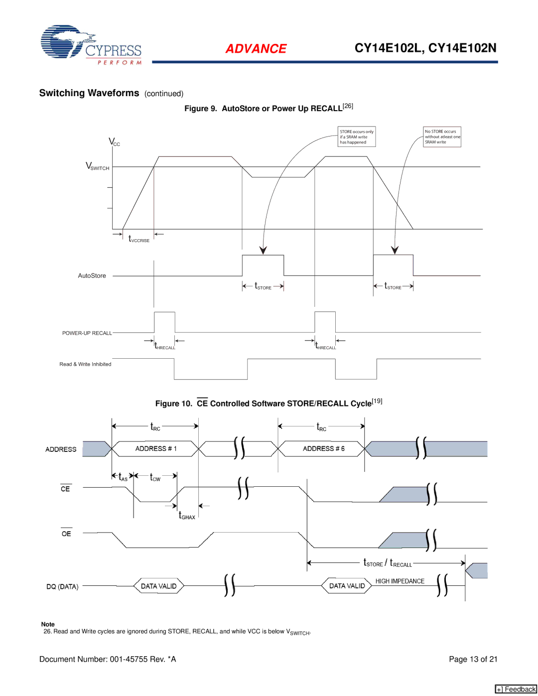
Switching Waveforms (continued)
Figure 9. AutoStore or Power Up RECALL[26]
| STORE occurs only | No STORE occurs | |
VCC | if a SRAM write | without atleast one | |
has happened | SRAM write | ||
|
VSWITCH |
|
tVCCRISE |
|
AutoStore | tSTORE |
tSTORE |
tHRECALL
tHRECALL
Read & Write Inhibited
Figure 10. CE Controlled Software STORE/RECALL Cycle[19]
Note
26. Read and Write cycles are ignored during STORE, RECALL, and while VCC is below VSWITCH.
Document Number: | Page 13 of 21 |
[+] Feedback