| | | | | ADVANCE | | CY14E102L, CY14E102N |
| | | | | | | | |
| | | | | | | |
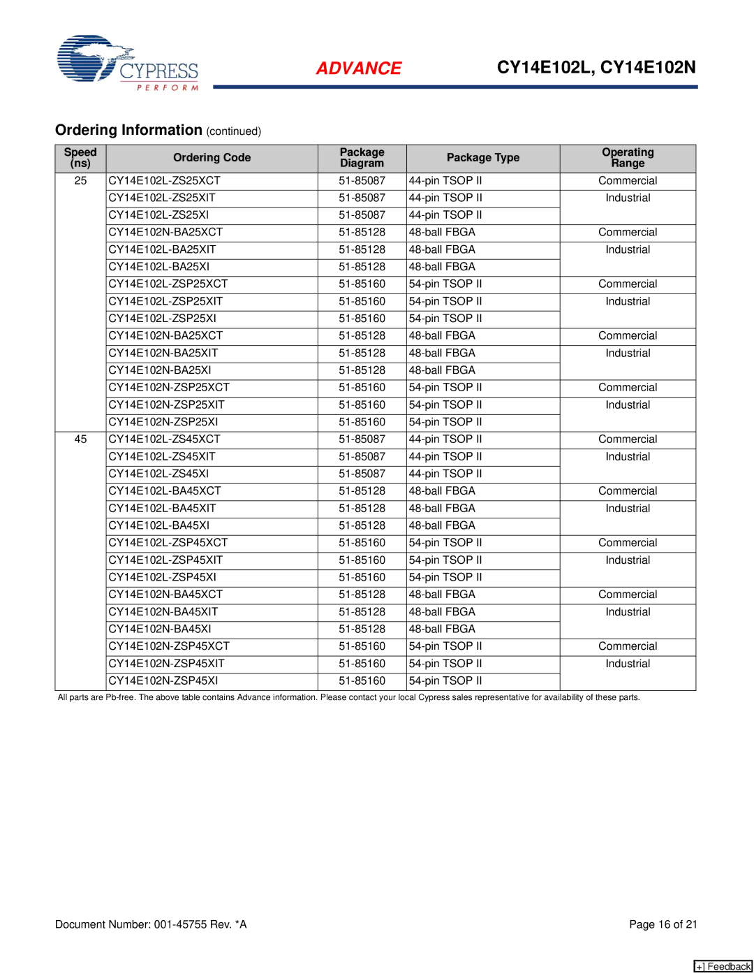
| Ordering Information (continued) | | | | |
| | | | | | | | |
| Speed | Ordering Code | Package | Package Type | Operating |
| (ns) | Diagram | Range |
| | | | | |
| 25 | CY14E102L-ZS25XCT | 51-85087 | 44-pin TSOP II | | Commercial |
| | | | | | |
| | CY14E102L-ZS25XIT | 51-85087 | 44-pin TSOP II | | Industrial |
| | | | | | |
| | CY14E102L-ZS25XI | 51-85087 | 44-pin TSOP II | | |
| | | | | | |
| | CY14E102N-BA25XCT | 51-85128 | 48-ball FBGA | | Commercial |
| | | | | | |
| | CY14E102L-BA25XIT | 51-85128 | 48-ball FBGA | | Industrial |
| | | | | | |
| | CY14E102L-BA25XI | 51-85128 | 48-ball FBGA | | |
| | | | | | |
| | CY14E102L-ZSP25XCT | 51-85160 | 54-pin TSOP II | | Commercial |
| | | | | | |
| | CY14E102L-ZSP25XIT | 51-85160 | 54-pin TSOP II | | Industrial |
| | | | | | |
| | CY14E102L-ZSP25XI | 51-85160 | 54-pin TSOP II | | |
| | | | | | |
| | CY14E102N-BA25XCT | 51-85128 | 48-ball FBGA | | Commercial |
| | | | | | |
| | CY14E102N-BA25XIT | 51-85128 | 48-ball FBGA | | Industrial |
| | | | | | |
| | CY14E102N-BA25XI | 51-85128 | 48-ball FBGA | | |
| | | | | | |
| | CY14E102N-ZSP25XCT | 51-85160 | 54-pin TSOP II | | Commercial |
| | | | | | |
| | CY14E102N-ZSP25XIT | 51-85160 | 54-pin TSOP II | | Industrial |
| | | | | | |
| | CY14E102N-ZSP25XI | 51-85160 | 54-pin TSOP II | | |
| | | | | | |
| 45 | CY14E102L-ZS45XCT | 51-85087 | 44-pin TSOP II | | Commercial |
| | | | | | |
| | CY14E102L-ZS45XIT | 51-85087 | 44-pin TSOP II | | Industrial |
| | | | | | |
| | CY14E102L-ZS45XI | 51-85087 | 44-pin TSOP II | | |
| | | | | | |
| | CY14E102L-BA45XCT | 51-85128 | 48-ball FBGA | | Commercial |
| | | | | | |
| | CY14E102L-BA45XIT | 51-85128 | 48-ball FBGA | | Industrial |
| | | | | | |
| | CY14E102L-BA45XI | 51-85128 | 48-ball FBGA | | |
| | | | | | |
| | CY14E102L-ZSP45XCT | 51-85160 | 54-pin TSOP II | | Commercial |
| | | | | | |
| | CY14E102L-ZSP45XIT | 51-85160 | 54-pin TSOP II | | Industrial |
| | | | | | |
| | CY14E102L-ZSP45XI | 51-85160 | 54-pin TSOP II | | |
| | | | | | |
| | CY14E102N-BA45XCT | 51-85128 | 48-ball FBGA | | Commercial |
| | | | | | |
| | CY14E102N-BA45XIT | 51-85128 | 48-ball FBGA | | Industrial |
| | | | | | |
| | CY14E102N-BA45XI | 51-85128 | 48-ball FBGA | | |
| | | | | | |
| | CY14E102N-ZSP45XCT | 51-85160 | 54-pin TSOP II | | Commercial |
| | | | | | |
| | CY14E102N-ZSP45XIT | 51-85160 | 54-pin TSOP II | | Industrial |
| | | | | | |
| | CY14E102N-ZSP45XI | 51-85160 | 54-pin TSOP II | | |
| | | | | | | | |
All parts are Pb-free. The above table contains Advance information. Please contact your local Cypress sales representative for availability of these parts.
Document Number: 001-45755 Rev. *A | Page 16 of 21 |