CY7C1215H
1-Mbit (32K x 32) Pipelined Sync SRAM
Features
•Registered inputs and outputs for pipelined operation
•32K × 32 common I/O architecture
•3.3V core power supply (VDD)
•2.5V/3.3V I/O power supply (VDDQ)
•Fast
— 3.5 ns (for
•Provide
•
Pentium® interleaved or linear burst sequences
•Separate processor and controller address strobes
•Synchronous
•Asynchronous output enable
•Offered in
•“ZZ” Sleep Mode Option
Functional Description[1]
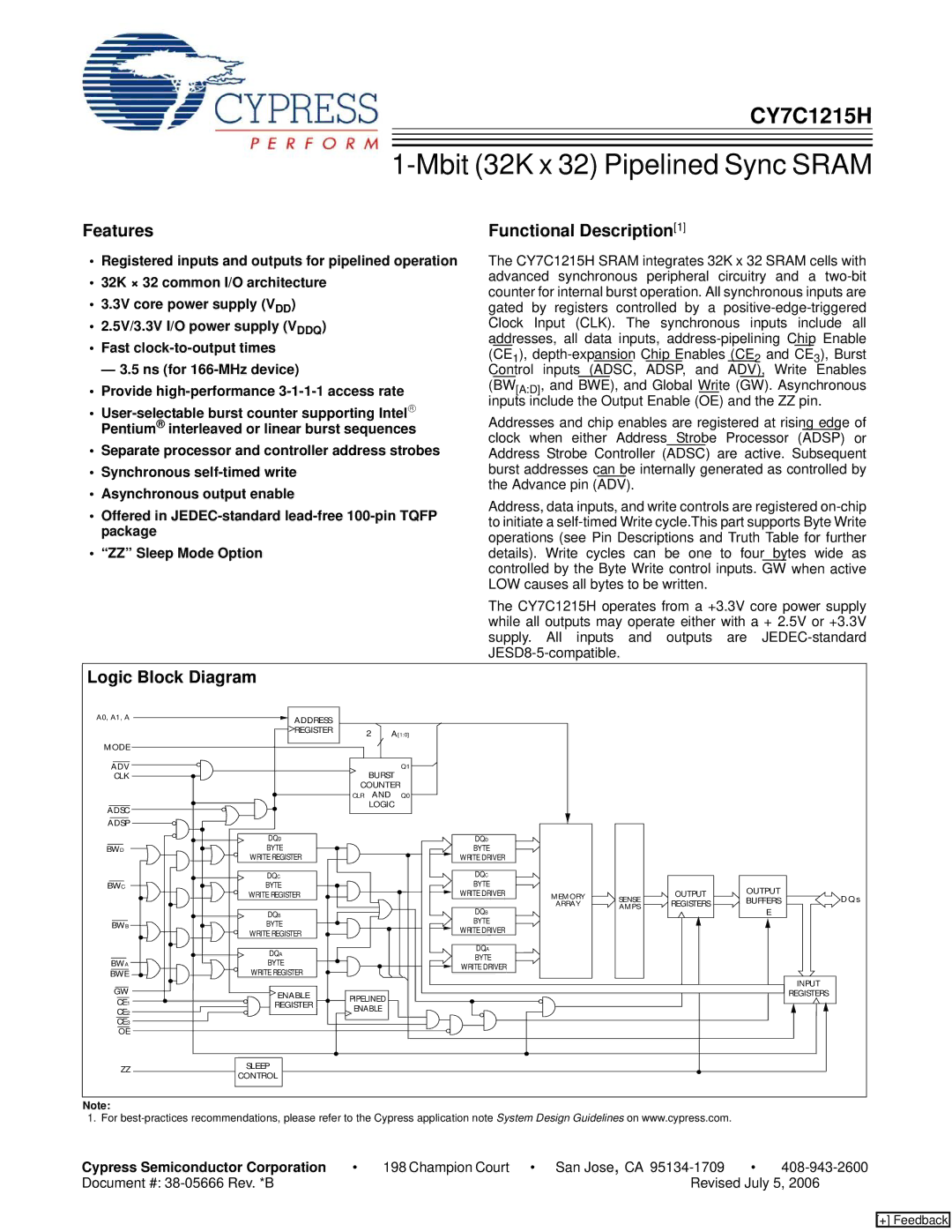
The CY7C1215H SRAM integrates 32K x 32 SRAM cells with advanced synchronous peripheral circuitry and a
Addresses and chip enables are registered at rising edge of clock when either Address Strobe Processor (ADSP) or Address Strobe Controller (ADSC) are active. Subsequent burst addresses can be internally generated as controlled by the Advance pin (ADV).
Address, data inputs, and write controls are registered
The CY7C1215H operates from a +3.3V core power supply while all outputs may operate either with a + 2.5V or +3.3V supply. All inputs and outputs are
Logic Block Diagram |
|
|
|
|
|
|
|
| |
A0, A1, A | ADDRESS |
|
|
|
|
|
|
|
|
|
|
|
|
|
|
|
|
| |
| REGISTER |
| 2 | A[1:0] |
|
|
|
|
|
|
|
|
|
|
|
|
| ||
MODE |
|
|
|
|
|
|
|
|
|
ADV |
|
|
| Q1 |
|
|
|
|
|
CLK |
|
| BURST |
|
|
|
|
| |
|
| COUNTER |
|
|
|
|
| ||
|
| CLR | AND | Q0 |
|
|
|
|
|
ADSC |
|
| LOGIC |
|
|
|
|
| |
|
|
|
|
|
|
|
|
| |
ADSP |
|
|
|
|
|
|
|
|
|
| DQD |
|
| DQD |
|
|
|
|
|
BWD | BYTE |
|
| BYTE |
|
|
|
|
|
| WRITE REGISTER |
|
| WRITE DRIVER |
|
|
|
|
|
| DQC |
|
| DQC |
|
|
|
|
|
BWC | BYTE |
|
| BYTE |
|
|
| OUTPUT |
|
| WRITE REGISTER |
|
| WRITE DRIVER | MEMORY | SENSE | OUTPUT | DQs | |
|
|
| BUFFERS | ||||||
|
|
|
|
| ARRAY | REGISTERS | |||
|
|
|
| DQB | AMPS | E |
| ||
| DQB |
|
|
|
|
| |||
|
|
|
|
|
|
| |||
BWB | BYTE |
|
| BYTE |
|
|
|
|
|
|
| WRITE DRIVER |
|
|
|
|
| ||
| WRITE REGISTER |
|
|
|
|
|
|
| |
|
|
|
|
|
|
|
|
| |
| DQA |
|
| DQA |
|
|
|
|
|
|
|
| BYTE |
|
|
|
|
| |
BWA | BYTE |
|
|
|
|
|
|
| |
|
| WRITE DRIVER |
|
|
|
|
| ||
BWE | WRITE REGISTER |
|
|
|
|
|
|
| |
|
|
|
|
|
|
|
| ||
GW |
|
|
|
|
|
|
|
| INPUT |
ENABLE | PIPELINED |
|
|
|
|
| REGISTERS | ||
CE1 | REGISTER |
|
|
|
|
|
| ||
ENABLE |
|
|
|
|
|
| |||
CE2 |
|
|
|
|
|
|
| ||
|
|
|
|
|
|
|
|
| |
CE3 |
|
|
|
|
|
|
|
|
|
OE |
|
|
|
|
|
|
|
|
|
ZZ | SLEEP |
|
|
|
|
|
|
|
|
CONTROL |
|
|
|
|
|
|
|
| |
|
|
|
|
|
|
|
|
| |
Note: |
|
|
|
|
|
|
|
|
|
1. For
Cypress Semiconductor Corporation | • | 198 Champion Court • San Jose, CA | • | |
Document #: |
| Revised July 5, 2006 | ||
[+] Feedback