CY7C1345G

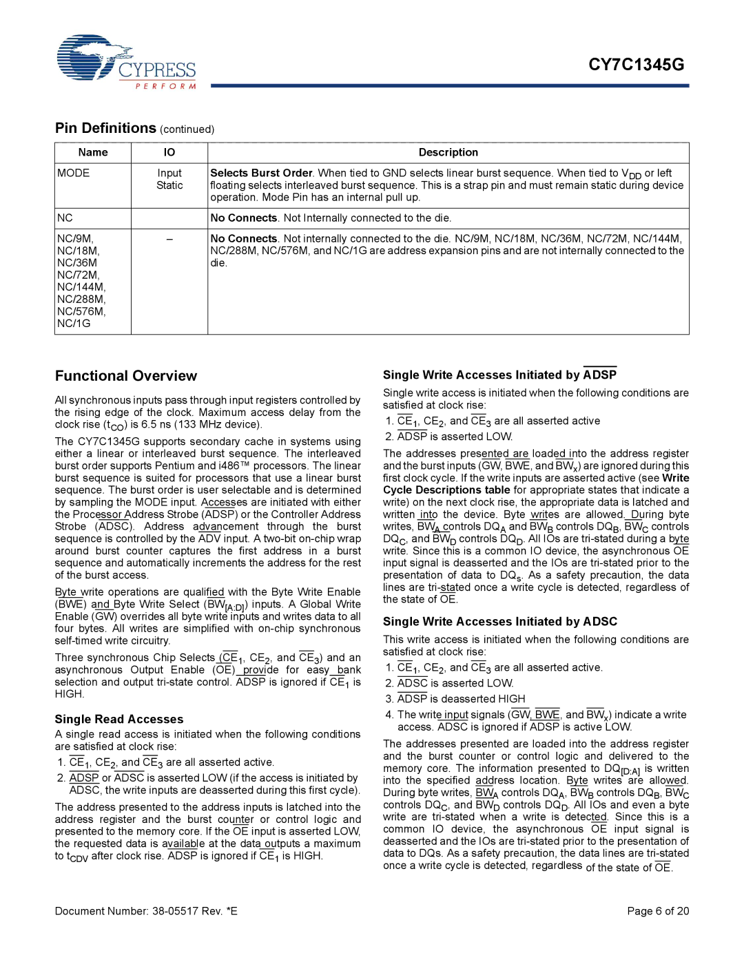
Pin Definitions (continued)

Name

IO

Description


MODE

Input

Selects Burst Order. When tied to GND selects linear burst sequence. When tied to VDD or left


Static

floating selects interleaved burst sequence. This is a strap pin and must remain static during device


operation. Mode Pin has an internal pull up.


NC


No Connects. Not Internally connected to the die.


NC/9M,

No Connects. Not internally connected to the die. NC/9M, NC/18M, NC/36M, NC/72M, NC/144M,

NC/18M,


NC/288M, NC/576M, and NC/1G are address expansion pins and are not internally connected to the

NC/36M


die.

NC/72M,


NC/144M,


NC/288M,


NC/576M,


NC/1G


Functional Overview

All synchronous inputs pass through input registers controlled by the rising edge of the clock. Maximum access delay from the clock rise (tCO) is 6.5 ns (133 MHz device).

The CY7C1345G supports secondary cache in systems using either a linear or interleaved burst sequence. The interleaved burst order supports Pentium and i486™ processors. The linear burst sequence is suited for processors that use a linear burst sequence. The burst order is user selectable and is determined by sampling the MODE input. Accesses are initiated with either the Processor Address Strobe (ADSP) or the Controller Address Strobe (ADSC). Address advancement through the burst sequence is controlled by the ADV input. A two-bit on-chip wrap around burst counter captures the first address in a burst sequence and automatically increments the address for the rest of the burst access.

Byte write operations are qualified with the Byte Write Enable (BWE) and Byte Write Select (BW[A:D]) inputs. A Global Write Enable (GW) overrides all byte write inputs and writes data to all four bytes. All writes are simplified with on-chip synchronous self-timed write circuitry.

Three synchronous Chip Selects (CE1, CE2, and CE3) and an asynchronous Output Enable (OE) provide for easy bank

selection and output tri-state control. ADSP is ignored if CE1 is HIGH.

Single Read Accesses

A single read access is initiated when the following conditions are satisfied at clock rise:

1.CE1, CE2, and CE3 are all asserted active.

2.ADSP or ADSC is asserted LOW (if the access is initiated by ADSC, the write inputs are deasserted during this first cycle).

The address presented to the address inputs is latched into the address register and the burst counter or control logic and presented to the memory core. If the OE input is asserted LOW, the requested data is available at the data outputs a maximum to tCDV after clock rise. ADSP is ignored if CE1 is HIGH.

Single Write Accesses Initiated by ADSP

Single write access is initiated when the following conditions are satisfied at clock rise:

1.CE1, CE2, and CE3 are all asserted active

2.ADSP is asserted LOW.

The addresses presented are loaded into the address register and the burst inputs (GW, BWE, and BWx) are ignored during this first clock cycle. If the write inputs are asserted active (see Write Cycle Descriptions table for appropriate states that indicate a write) on the next clock rise, the appropriate data is latched and written into the device. Byte writes are allowed. During byte writes, BWA controls DQA and BWB controls DQB, BWC controls DQC, and BWD controls DQD. All IOs are tri-stated during a byte write. Since this is a common IO device, the asynchronous OE input signal is deasserted and the IOs are tri-stated prior to the presentation of data to DQs. As a safety precaution, the data lines are tri-stated once a write cycle is detected, regardless of the state of OE.

Single Write Accesses Initiated by ADSC

This write access is initiated when the following conditions are satisfied at clock rise:

1.CE1, CE2, and CE3 are all asserted active.

2.ADSC is asserted LOW.

3.ADSP is deasserted HIGH

4.The write input signals (GW, BWE, and BWx) indicate a write access. ADSC is ignored if ADSP is active LOW.

The addresses presented are loaded into the address register and the burst counter or control logic and delivered to the memory core. The information presented to DQ[D:A] is written into the specified address location. Byte writes are allowed. During byte writes, BWA controls DQA, BWB controls DQB, BWC controls DQC, and BWD controls DQD. All IOs and even a byte write are tri-stated when a write is detected. Since this is a common IO device, the asynchronous OE input signal is deasserted and the IOs are tri-stated prior to the presentation of data to DQs. As a safety precaution, the data lines are tri-stated once a write cycle is detected, regardless of the state of OE.

Document Number: 38-05517 Rev. *E

Page 6 of 20

Page 6
Image 6
Cypress CY7C1345G manual Functional Overview, Static, Operation. Mode Pin has an internal pull up

CY7C1345G specifications

The Cypress CY7C1345G is a high-performance static random-access memory (SRAM) device designed for various applications requiring fast data access and minimal power consumption. As a member of Cypress's prolific family of SRAMs, the CY7C1345G is particularly noted for its performance in networking and telecommunications.

This device features a 512 Kbit (64 K x 8) memory organization, making it suitable for applications needing moderate amounts of fast-access memory. The CY7C1345G operates at a wide voltage range of 2.7V to 3.6V, accommodating both high-performance and low-power applications. One of its standout attributes is its fast access time, with read cycle times as low as 10 ns, allowing for rapid data retrieval that is essential for modern computing requirements.

Another key feature of the CY7C1345G is its low-power operation mode, making it an excellent choice for battery-operated applications. It has a typical active current of only 35 mA and a standby current of just 3 µA, ensuring prolonged battery life while still maintaining high-performance levels. This low power consumption is complemented by the device's sleep mode functionality, which further reduces power draw during periods of inactivity.

In terms of interface, the CY7C1345G employs a simple asynchronous access protocol, ensuring ease of integration into existing systems without the need for complex timing schemes. The device supports asynchronous read and write operations, with an output enable feature that facilitates efficient data retrieval.

The CY7C1345G is encased in a compact 44-pin TSOP II package, making it suitable for applications where space constraints are critical. Its design adheres to rigorous quality and reliability standards, with the device being fully tested to meet JEDEC specifications.

With its blend of speed, low power consumption, and simple interface, the Cypress CY7C1345G SRAM is ideal for a wide array of applications, including telecommunications systems, networking devices, and embedded systems. As technology drives the demand for faster and more efficient memory solutions, the CY7C1345G stands out as a reliable and versatile choice in the SRAM landscape.