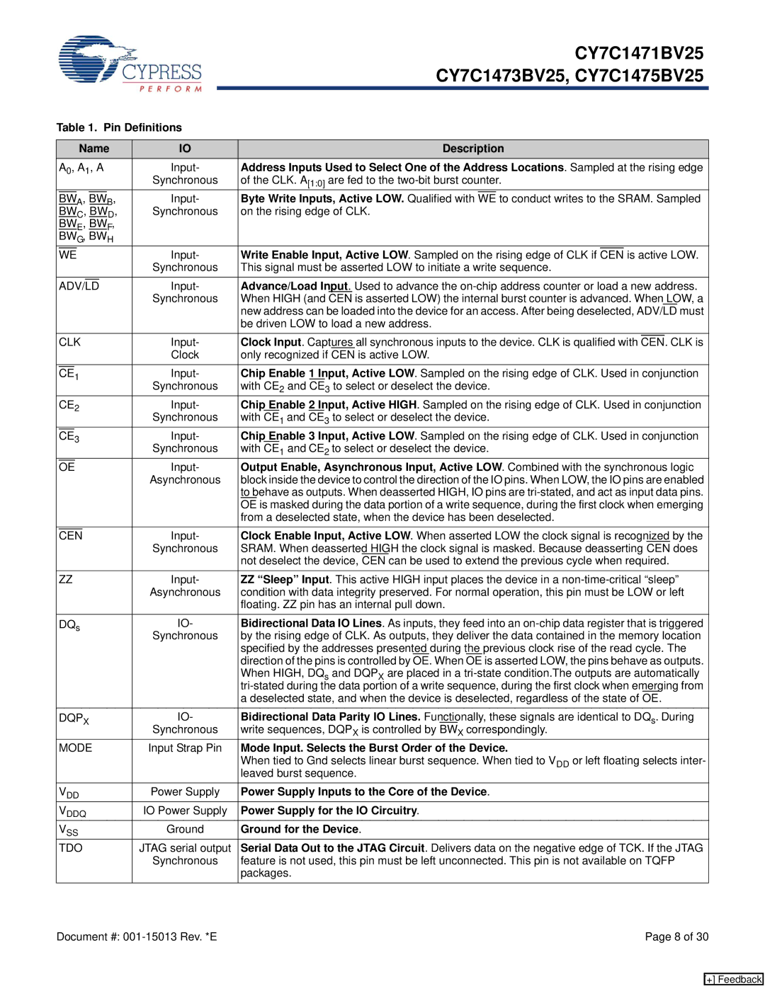
Cypress CY7C1475BV25 manual Pin Definitions Name Description, Power Supply for the IO Circuitry

Models: CY7C1475BV25 CY7C1473BV25 CY7C1471BV25

1 30
Download 30 pages 32.83 Kb
Page 8
Image 8


CY7C1471BV25


CY7C1473BV25, CY7C1475BV25


Table 1. Pin Definitions


Name

IO

Description


A0, A1, A

Input-

Address Inputs Used to Select One of the Address Locations. Sampled at the rising edge


Synchronous

of the CLK. A[1:0] are fed to the two-bit burst counter.


A,


B,

Input-

Byte Write Inputs, Active LOW. Qualified with


to conduct writes to the SRAM. Sampled


BW

BW

WE


BWC, BWD,

Synchronous

on the rising edge of CLK.


BWE, BWF,


BWG, BWH


Input-

Write Enable Input, Active LOW. Sampled on the rising edge of CLK if


is active LOW.


WE

CEN


Synchronous

This signal must be asserted LOW to initiate a write sequence.


Input-

Advance/Load Input. Used to advance the on-chip address counter or load a new address.


ADV/LD


Synchronous

When HIGH (and CEN is asserted LOW) the internal burst counter is advanced. When LOW, a


new address can be loaded into the device for an access. After being deselected, ADV/LD must


be driven LOW to load a new address.


CLK

Input-

Clock Input. Captures all synchronous inputs to the device. CLK is qualified with


CLK is


CEN.


Clock

only recognized if CEN is active LOW.


1


Input-

Chip Enable 1 Input, Active LOW. Sampled on the rising edge of CLK. Used in conjunction


CE


Synchronous

with CE2 and CE3 to select or deselect the device.


CE2

Input-

Chip Enable 2 Input, Active HIGH. Sampled on the rising edge of CLK. Used in conjunction


Synchronous

with CE1 and CE3 to select or deselect the device.


3


Input-

Chip Enable 3 Input, Active LOW. Sampled on the rising edge of CLK. Used in conjunction


CE


Synchronous

with CE1 and CE2 to select or deselect the device.


Input-

Output Enable, Asynchronous Input, Active LOW. Combined with the synchronous logic


OE


Asynchronous

block inside the device to control the direction of the IO pins. When LOW, the IO pins are enabled


to behave as outputs. When deasserted HIGH, IO pins are tri-stated, and act as input data pins.


OE is masked during the data portion of a write sequence, during the first clock when emerging


from a deselected state, when the device has been deselected.


Input-

Clock Enable Input, Active LOW. When asserted LOW the clock signal is recognized by the


CEN


Synchronous

SRAM. When deasserted HIGH the clock signal is masked. Because deasserting CEN does


not deselect the device, CEN can be used to extend the previous cycle when required.


ZZ

Input-

ZZ “Sleep” Input. This active HIGH input places the device in a non-time-critical “sleep”


Asynchronous

condition with data integrity preserved. For normal operation, this pin must be LOW or left


floating. ZZ pin has an internal pull down.


DQs

IO-

Bidirectional Data IO Lines. As inputs, they feed into an on-chip data register that is triggered


Synchronous

by the rising edge of CLK. As outputs, they deliver the data contained in the memory location


specified by the addresses presented during the previous clock rise of the read cycle. The


direction of the pins is controlled by OE. When OE is asserted LOW, the pins behave as outputs.


When HIGH, DQs and DQPX are placed in a tri-state condition.The outputs are automatically


tri-stated during the data portion of a write sequence, during the first clock when emerging from


a deselected state, and when the device is deselected, regardless of the state of OE.


DQPX

IO-

Bidirectional Data Parity IO Lines. Functionally, these signals are identical to DQs. During


Synchronous

write sequences, DQPX is controlled by BWX correspondingly.


MODE

Input Strap Pin

Mode Input. Selects the Burst Order of the Device.


When tied to Gnd selects linear burst sequence. When tied to VDD or left floating selects inter-


leaved burst sequence.


VDD

Power Supply

Power Supply Inputs to the Core of the Device.


VDDQ

IO Power Supply

Power Supply for the IO Circuitry.


VSS

Ground

Ground for the Device.


TDO

JTAG serial output

Serial Data Out to the JTAG Circuit. Delivers data on the negative edge of TCK. If the JTAG


Synchronous

feature is not used, this pin must be left unconnected. This pin is not available on TQFP


packages.

Document #: 001-15013 Rev. *E


Page 8 of 30

[+] Feedback

Page 8
Image 8
Cypress CY7C1475BV25, CY7C1471BV25 manual Pin Definitions Name Description, Byte Write Inputs, Active LOW. Qualified with