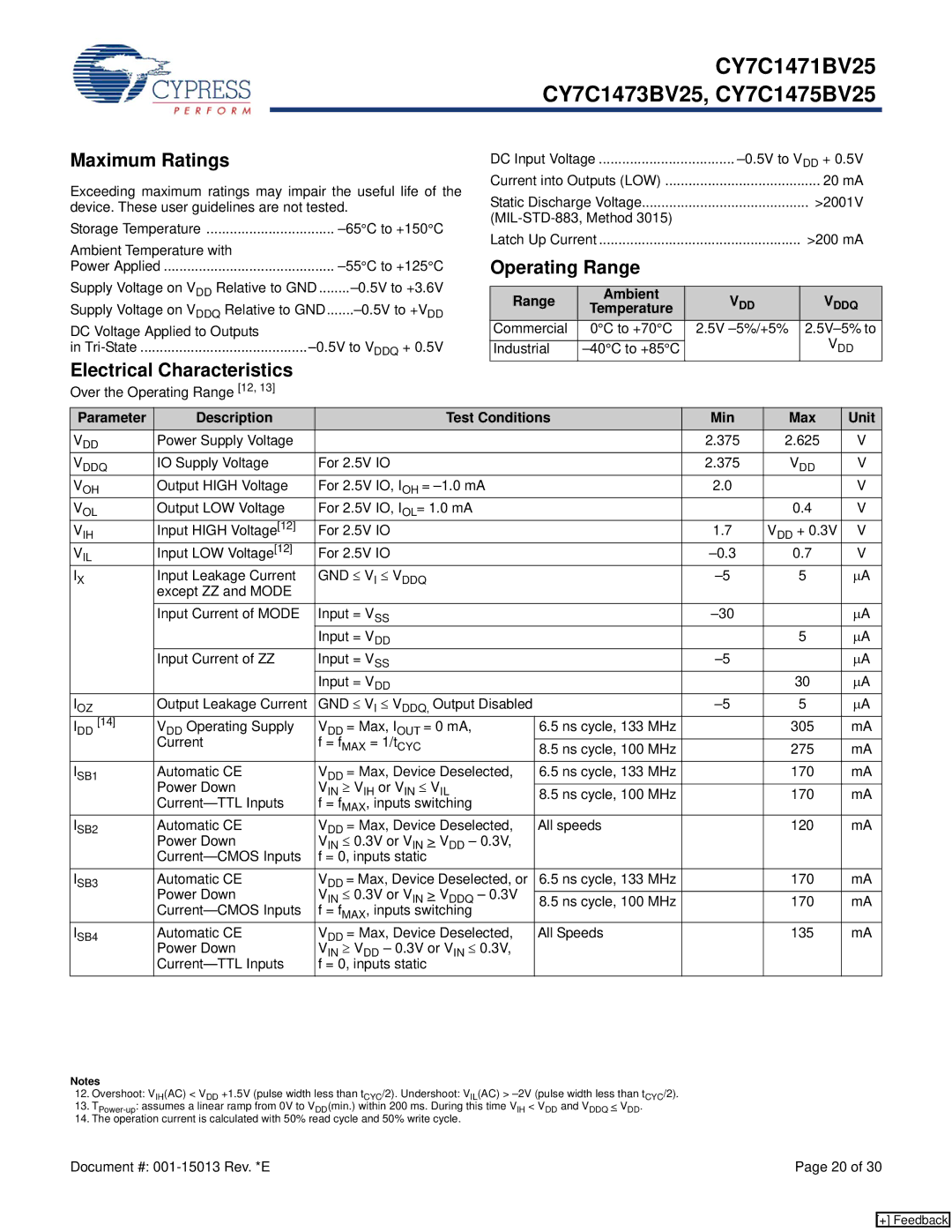
CY7C1475BV25, CY7C1473BV25, CY7C1471BV25 specifications
Cypress Semiconductor, a leader in specialized memory solutions, offers a range of high-performance SRAM products, including the CY7C1471BV25, CY7C1473BV25, and CY7C1475BV25. These devices are designed to provide high-speed data processing capabilities along with impressive power efficiency, making them ideal choices for a variety of applications in telecommunications, networking, automotive, and consumer electronics.The CY7C1471BV25 features a 1-Mbit density, while the CY7C1473BV25 and CY7C1475BV25 support densities of 3-Mbits and 5-Mbits respectively. All three models utilize a 3.3V power supply, and deliver fast access times of 5 ns (for CY7C1471BV25) and 6 ns (for CY7C1473BV25 and CY7C1475BV25). This rapid access enables quicker data retrieval and overall enhanced system performance.
One of the standout features of these SRAM devices is their asynchronous operation, which allows for straightforward integration into existing systems without the need for complex timing protocols. They can be easily interfaced with various microcontrollers and digital signal processors, providing flexibility and ease of use. Additionally, the devices are available in multiple package options, including the widely used TSOP and BGA formats, enabling designers to choose the best fit for their specific layouts.
In terms of technology, these SRAMs leverage advanced CMOS manufacturing processes, which contribute to their low power consumption and high reliability. With sleep modes and low standby current, they are particularly suited for battery-operated devices that demand energy efficiency.
Cypress products are renowned for their reliability and robustness, ensuring that the CY7C1471BV25, CY7C1473BV25, and CY7C1475BV25 can withstand the demands of harsh environments and extended usage. The devices also incorporate features such as high-speed data ports, which facilitate bidirectional data flow, making them optimal for both read and write operations.
In summary, the CY7C1471BV25, CY7C1473BV25, and CY7C1475BV25 SRAMs by Cypress are excellent choices for those seeking high-performance, low-power memory solutions. Their advanced technology, combined with a variety of features and options, caters to the needs of many industries, paving the way for innovative designs in modern electronics.

