CY7C1392CV18, CY7C1992CV18 CY7C1393CV18, CY7C1394CV18
synchronized to the output clock of the
DLL
These chips use a Delay Lock Loop (DLL) that is designed to function between 120 MHz and the specified maximum clock frequency. During power up, when the DOFF is tied HIGH, the
DLL is locked after 1024 cycles of stable clock. The DLL can also be reset by slowing or stopping the input clocks K and K for a minimum of 30 ns. However, it is not necessary to reset the DLL to lock it to the desired frequency. The DLL automatically locks 1024 clock cycles after a stable clock is presented. The DLL may be disabled by applying ground to the DOFF pin. When the DLL is turned off, the device behaves in
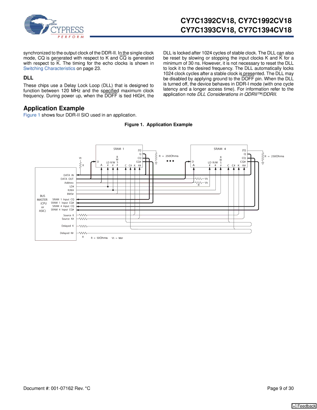
Application Example
Figure 1 shows four DDR-II SIO used in an application.
Figure 1. Application Example
| DATA IN | |
| DATA OUT | |
| Address | |
| LD# | |
| R/W# | |
BUS | BWS# | |
| ||
MASTER | SRAM 1 Input CQ | |
(CPU | SRAM 1 Input CQ# | |
or | SRAM 4 Input CQ | |
SRAM 4 Input CQ# | ||
ASIC) | ||
| ||
| Source K | |
| Source K# | |
| Delayed K | |
| Delayed K# |
|
|
| SRAM 1 |
|
|
| ZQ |
|
| SRAM 4 |
|
|
| ZQ | ||
|
|
|
|
|
|
|
|
|
|
|
|
|
|
| ||
|
|
|
| B |
|
|
| Q | R = 250Ohms |
|
| B |
|
|
| Q |
Vt |
|
|
|
|
|
| CQ |
|
|
|
|
| CQ | |||
|
|
| W |
|
|
|
|
|
| W |
|
|
| |||
| D | LD R/W | B |
|
|
| CQ# | D | LD R/W |
|
|
| CQ# | |||
| S |
|
|
| S |
|
|
| ||||||||
R | A | LD R/W W |
|
|
|
| A | # | # | # |
|
|
|
| ||
# | # | # | C | C# | K | K# | C | C# | K | K# | ||||||
|
| # | # | # |
|
|
|
| ||||||||
|
|
|
|
|
|
|
|
|
| Vt |
|
|
|
|
|
|
|
|
|
|
|
|
|
|
|
| Vt |
|
|
|
|
|
|
|
|
|
|
|
|
|
|
|
| R |
|
|
|
|
|
|
R | R = 50Ohms | Vt = VREF |
|
|
|
|
|
|
|
|
|
|
|
| ||
R = 250Ohms
Document #: | Page 9 of 30 |
[+] Feedback