CY7C1392CV18, CY7C1992CV18
CY7C1393CV18, CY7C1394CV18
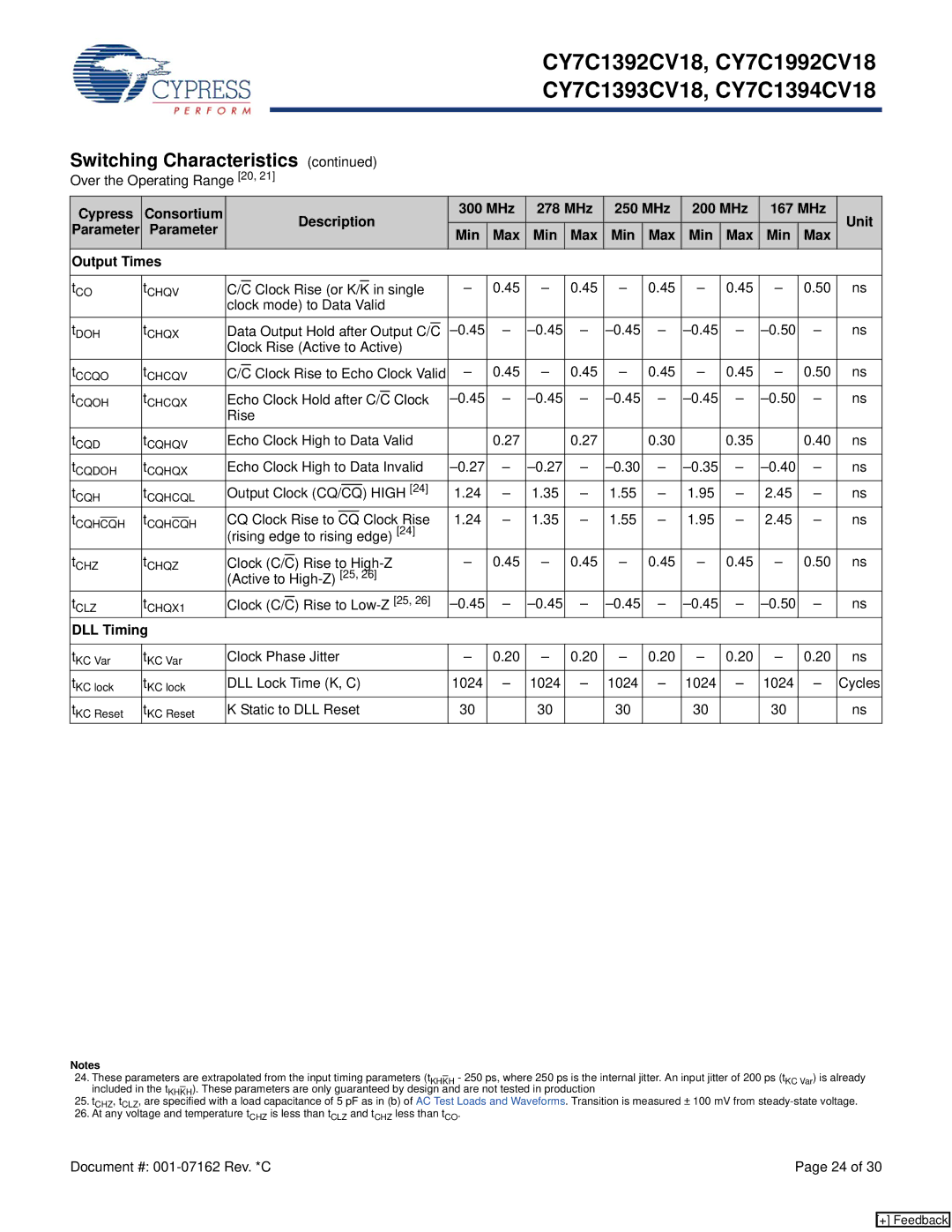
Switching Characteristics (continued)
Over the Operating Range [20, 21]
Cypress | Consortium |
|
|
|
|
| Description | 300 MHz | 278 MHz | 250 MHz | 200 MHz | 167 MHz | Unit | ||||||||||||||||
Parameter | Parameter |
|
|
|
|
| Min | Max | Min | Max | Min | Max | Min | Max | Min | Max | |||||||||||||
|
|
|
|
|
|
|
|
|
|
|
|
|
|
|
| ||||||||||||||
|
|
|
|
|
|
|
|
|
|
|
|
|
|
|
|
|
|
|
| ||||||||||
Output Times |
|
|
|
|
|
|
|
|
|
|
|
|
|
|
|
|
|
|
|
|
|
|
|
|
|
| |||
|
|
|
|
|
|
|
|
|
|
|
|
|
|
|
|
|
|
|
|
|
|
|
|
|
|
| |||
tCO | tCHQV | C/C | Clock Rise (or K/K in single | – | 0.45 | – | 0.45 | – | 0.45 | – | 0.45 | – | 0.50 | ns | |||||||||||||||
|
|
|
| clock mode) to Data Valid |
|
|
|
|
|
|
|
|
|
|
| ||||||||||||||
tDOH | tCHQX |
|
|
|
|
|
|
|
|
|
|
|
|
|
|
| – | – | – | – | – | ns | |||||||
Data Output Hold after Output C/C |
| ||||||||||||||||||||||||||||
|
|
|
| Clock Rise (Active to Active) |
|
|
|
|
|
|
|
|
|
|
| ||||||||||||||
tCCQO | tCHCQV |
|
| Clock Rise to Echo Clock Valid | – | 0.45 | – | 0.45 | – | 0.45 | – | 0.45 | – | 0.50 | ns | ||||||||||||||
C/C | |||||||||||||||||||||||||||||
tCQOH | tCHCQX |
|
|
|
|
|
|
|
|
|
|
|
| Clock | – | – | – | – | – | ns | |||||||||
Echo Clock Hold after C/C | |||||||||||||||||||||||||||||
|
|
|
| Rise |
|
|
|
|
|
|
|
|
|
|
| ||||||||||||||
tCQD | tCQHQV | Echo Clock High to Data Valid |
| 0.27 |
| 0.27 |
| 0.30 |
| 0.35 |
| 0.40 | ns | ||||||||||||||||
tCQDOH | tCQHQX | Echo Clock High to Data Invalid | – | – | – | – | – | ns | |||||||||||||||||||||
tCQH | tCQHCQL |
|
|
|
|
|
|
|
|
| HIGH [24] | 1.24 | – | 1.35 | – | 1.55 | – | 1.95 | – | 2.45 | – | ns | |||||||
Output Clock (CQ/CQ) | |||||||||||||||||||||||||||||
tCQHCQH |
| tCQHCQH |
| CQ Clock Rise to |
|
| Clock Rise | 1.24 | – | 1.35 | – | 1.55 | – | 1.95 | – | 2.45 | – | ns | |||||||||||
|
| CQ | |||||||||||||||||||||||||||
|
|
|
| (rising edge to rising edge) [24] |
|
|
|
|
|
|
|
|
|
|
| ||||||||||||||
tCHZ | tCHQZ |
|
|
|
|
| Rise to | – | 0.45 | – | 0.45 | – | 0.45 | – | 0.45 | – | 0.50 | ns | |||||||||||
Clock (C/C) | |||||||||||||||||||||||||||||
|
|
|
| (Active to |
|
|
|
|
|
|
|
|
|
|
| ||||||||||||||
tCLZ | tCHQX1 |
|
|
|
|
| Rise to | – | – | – | – | – | ns | ||||||||||||||||
Clock (C/C) | |||||||||||||||||||||||||||||
DLL Timing |
|
|
|
|
|
|
|
|
|
|
|
|
|
|
|
|
|
|
|
|
|
|
|
|
|
| |||
|
|
|
|
|
|
|
|
|
|
|
|
|
| ||||||||||||||||
tKC Var | tKC Var | Clock Phase Jitter | – | 0.20 | – | 0.20 | – | 0.20 | – | 0.20 | – | 0.20 | ns | ||||||||||||||||
tKC lock | tKC lock | DLL Lock Time (K, C) | 1024 | – | 1024 | – | 1024 | – | 1024 | – | 1024 | – | Cycles | ||||||||||||||||
tKC Reset | tKC Reset | K Static to DLL Reset | 30 |
| 30 |
| 30 |
| 30 |
| 30 |
| ns | ||||||||||||||||
Notes
24.These parameters are extrapolated from the input timing parameters (tKHKH - 250 ps, where 250 ps is the internal jitter. An input jitter of 200 ps (tKC Var) is already included in the tKHKH). These parameters are only guaranteed by design and are not tested in production
25.tCHZ, tCLZ, are specified with a load capacitance of 5 pF as in (b) of AC Test Loads and Waveforms. Transition is measured ± 100 mV from
26.At any voltage and temperature tCHZ is less than tCLZ and tCHZ less than tCO.
Document #: | Page 24 of 30 |
[+] Feedback