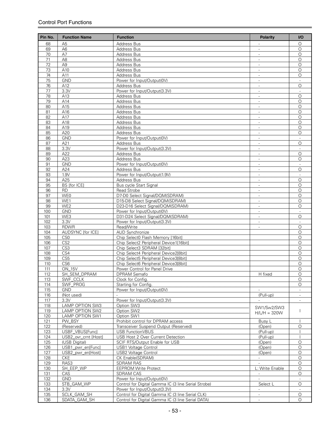
LC-X71 LC-X71L specifications
The Eiki LC-X71 and LC-X71L are advanced multimedia projectors designed for a range of applications, from education to corporate environments. Known for their outstanding image quality and impressive clarity, these projectors combine technological innovation with user-friendly features, making them ideal for presentations, lectures, and various visual displays.One of the defining characteristics of the LC-X71 series is its high brightness output. With 6000 ANSI lumens, these projectors ensure clear and vibrant images, even in well-lit rooms. This level of brightness is complemented by a native XGA resolution (1024 x 768), providing sharp details and vivid colors. The LC-X71L model features a slightly enhanced brightness, making it suitable for larger venues or where ambient light cannot be controlled.
The Eiki LC-X71 and LC-X71L utilize a DLP (Digital Light Processing) technology that enhances color accuracy and contrast. This technology minimizes the visibility of pixels, ensuring smooth images that remain sharp at various viewing distances. Moreover, the projectors incorporate a high contrast ratio, which contributes to deep blacks and bright whites, making them perfect for presentations with complex graphics.
Another noteworthy feature is the flexible connectivity options. The LC-X71 series offers multiple input terminals, including HDMI, VGA, and USB, allowing for seamless integration with various devices, from laptops to video players. This versatility enables users to easily switch between different content sources. Additionally, the projectors support wireless presentation capability, enhancing user convenience and reducing the clutter of cables.
User convenience doesn’t stop at connectivity. The LC-X71 and LC-X71L are designed for easy installation and maintenance. Their lightweight design and compact dimensions facilitate portability, making them easy to move between locations. They also feature a filter-free design, reducing maintenance efforts and ensuring long-term reliability.
In terms of energy efficiency, both models are equipped with Eco Mode, which extends lamp life and reduces power consumption. The lamp life can reach up to 4000 hours, depending on usage, making it a cost-effective solution for prolonged use.
In conclusion, the Eiki LC-X71 and LC-X71L projectors deliver exceptional performance, combining high brightness, versatile connectivity, and user-friendly features. Their technological advancements cater to various needs, ensuring that they stand out in the competitive market of multimedia projectors.
