Victoreen 875
Operators Manual
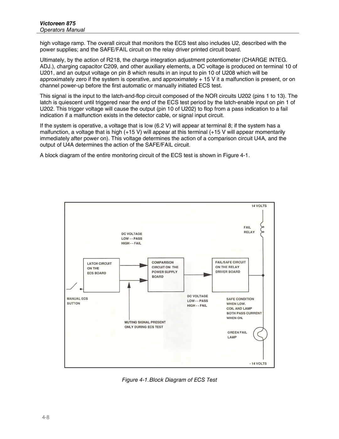
high voltage ramp. The overall circuit that monitors the ECS test also includes U2, described with the power supplies; and the SAFE/FAIL circuit on the relay driver printed circuit board.
Ultimately, by the action of R218, the charge integration adjustment potentiometer (CHARGE INTEG. ADJ.), charging capacitor C209, and other auxiliary elements, a DC voltage is produced on terminal 10 of U201, and an output voltage on pin 8 which results in an input to pin 10 of U208 which will be approximately zero if the system is operative, and approximately + 15 V it a malfunction is present, or on channel
This signal is the input to the
If the system is operative, a voltage that is low (6.2 V) will appear at terminal 8; if the system has a malfunction, a voltage that is high (+15 V) will appear at this terminal (+15 V will appear momentarily immediately after power on). This voltage determines the action of a comparison circuit U4A, and the output of U4A determines the action of the SAFE/FAIL circuit.
A block diagram of the entire monitoring circuit of the ECS test is shown in Figure