Main
Page
Contents
Page
Page
Page
8 Enhanced Serial AUDIO Interface (ESAI) . . . . . . . . . . . . . . . . . . . . . . . . . . .8-1
Page
Page
9 Enhanced Serial Audio Interface 1 (ESAI_1) . . . . . . . . . . . . . . . . . . . . . . . . .9-1
Page
Page
Page
Page
List of Figures
Page
Page
Page
List of Tables
Page
Preface
Manual Conventions
Page
Page
Freescale Semiconductor 1-1
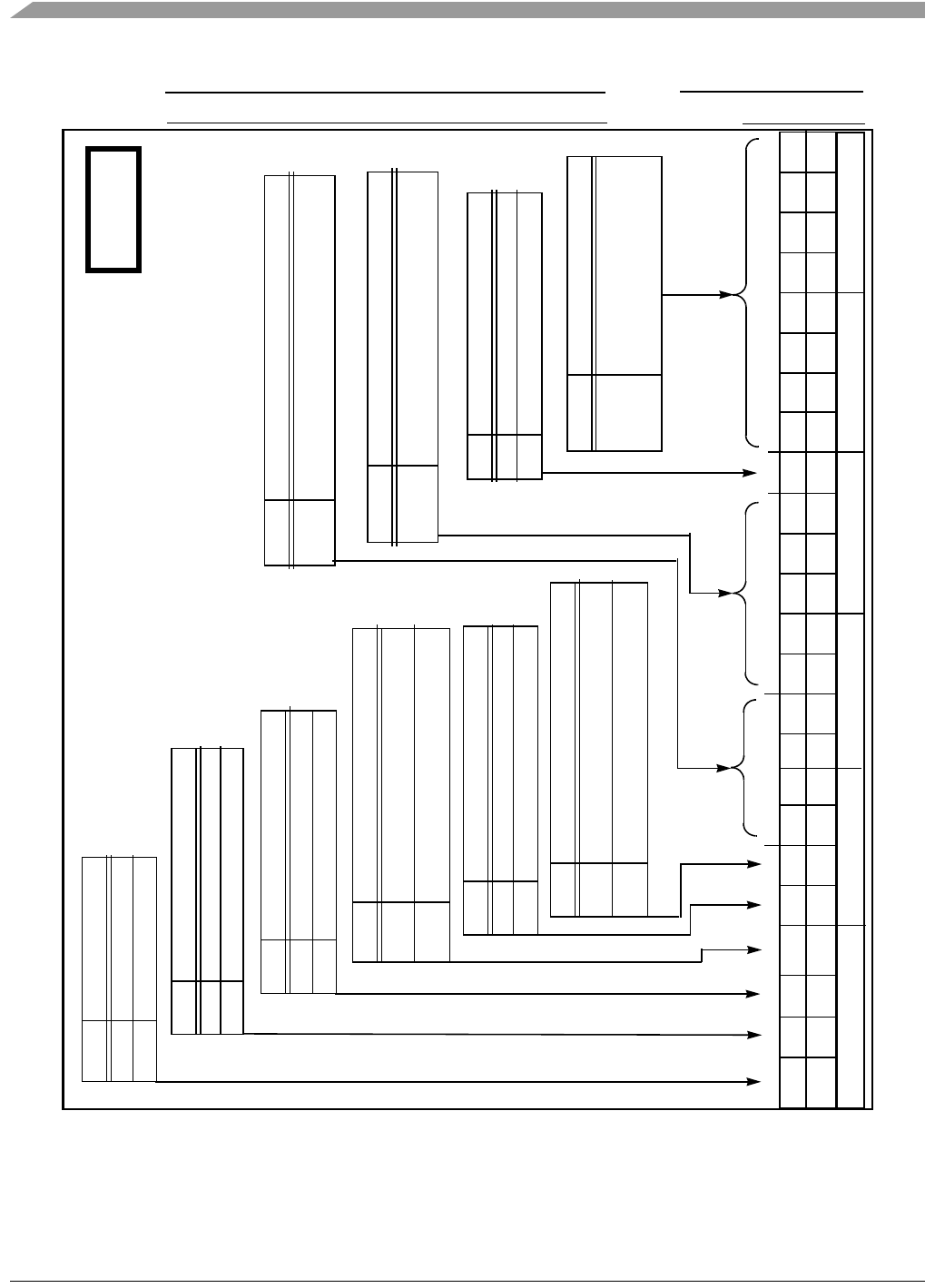
1 DSP56366 Overview
1.1 Introduction
Figure 1-1 DSP56366 Block Diagram
MEMORY EXPANSION AREA
PERIPHERAL
1.2 DSP56300 Core Description
1.3 DSP56366 Audio Processor Architecture
1.4 DSP56300 Core Functional Blocks
1.4.1 Data ALU
1.4.1.1 Data ALU Registers
1.4.1.2 Multiplier-Accumulator (MAC)
1.4.2 Address Generation Unit (AGU)
1.4.3 Program Control Unit (PCU)
1.4.4 Internal Buses
1.4.5 Direct Memory Access (DMA)
1.4.6 PLL-based Clock Oscillator
1.4.7 JTAG TAP and OnCE Module
1.4.8 On-Chip Memory
1.4.9 Off-Chip Memory Expansion
1.5 Peripheral Overview
1.5.1 Host Interface (HDI08)
1.5.2 General Purpose Input/Output (GPIO)
1.5.3 Triple Timer (TEC)
1.5.4 Enhanced Serial Audio Interface (ESAI)
1.5.5 Enhanced Serial Audio Interface 1 (ESAI_1)
1.5.6 Serial Host Interface (SHI)
1.5.7 Digital Audio Transmitter (DAX)
2 Signal/Connection Descriptions
2.1 S ignal Groupings
DSP56366
2.2 Power
2.3 Ground
Table2-2 Power Inputs
Table2-3 Grounds
2.4 Clock and PLL
Table2-4 Clock and PLL Signals
Table2-3 Grounds (continued)
2.5 E xternal Memory Expansion Port (Port A)
2.5.3 External Bus Control
2.5.1 External Address Bus
2.5.2 External Data Bus
Table2-5 External Address Bus Signals
Table2-7 External Bus Control Signals (continued)
2.6 Interrupt and Mode Control
Table2-7 External Bus Control Signals (continued)
Table2-8 Interrupt and Mode Control
2.7 PARALLEL HOST INTERFACE (HDI08)
Table2-9 Host Interface
Page
Page
2.8 Serial Host Interface
Table2-10 Serial Host Interface Signals
Page
Table2-10 Serial Host Interface Signals (continued)
2.9 E nhanced Serial Audio Interface
Table2-11 Enhanced Serial Audio Interface Signals
Page
Page
Page
2.10 Enhanced Serial Audio Interface_1
Table2-12 Enhanced Serial Audio Interface_1 Signals
Table2-12 Enhanced Serial Audio Interface_1 Signals (continued)
2.11 SPDIF Transmitter Digital Audio Interface
Table2 -13 Digital Audio Interface (DAX) Signals
Table2-12 Enhanced Serial Audio Interface_1 Signals (continued)
2.12 Timer
2.13 JTAG/OnCE Interface
Table2-14 Timer Signal
Table2-15 JTAG/OnCE Interface
3 Memory Configuration
3.1 Data and Program Memory Maps
Table3-1 Internal Memory Configurations
Table3-2 On-chip RAM Memory Locations
Table3-3 On-chip ROM Memory Locations
Freescale Semiconductor 3-3
Figure 3-1 Memory Maps for MSW=(X,X), CE=0, MS=0, SC=0
Figure 3-2 Memory Maps for MSW=(X,X), CE=1, MS=0, SC=0
3-4 Freescale Semiconductor
Figure 3-3 Memory Maps for MSW=(0,0), CE=0 MS=1, SC=0
Figure 3-4 Memory Maps for MSW=(0,1), CE=0, MS=1, SC=0
Freescale Semiconductor 3-5
Figure 3-5 Memory Maps for MSW=(1,0), CE=0, MS=1, SC=0
Figure 3-6 Memory Maps for MSW=(0,0), CE=1, MS=1, SC=0
3-6 Freescale Semiconductor
Figure 3-7 Memory Maps for MSW=(0,1), CE=1, MS=1, SC=0
Figure 3-8 Memory Maps for MSW=(1,0), CE=1, MS=1, SC=0
DSP56366 24-Bit Digital Signal Processor User Manual, Rev. 4 Freescale Semiconductor 3-7
Figure 3-9 Memory Maps for MSW=(X,X), CE=0, MS=0, SC=1
Figure 3-10 Memory Maps for MSW=(X,X), CE=1, MS=0, SC=1
3-8 Freescale Semiconductor
Figure 3-11 Memory Maps for MSW=(0,0), CE=0, MS=1, SC=1
Figure 3-12 Memory Maps for MSW=(0,1), CE=0, MS=1, SC=1
Freescale Semiconductor 3-9
Figure 3-13 Memory Maps for MSW=(1,0), CE=0, MS=1, SC=1
Figure 3-14 Memory Maps for MSW=(0,0), CE=1, MS=1, SC=1
DSP56366 24-Bit Digital Signal Processor User Manual, Rev. 4 3-10 Freescale Semiconductor
Figure 3-15 Memory Maps for MSW=(0,1), CE=1, MS=1, SC=1
Figure 3-16 Memory Maps for MSW=(1,0), CE=1, MS=1, SC=1
3.1.1 Reserved Memory Spaces
3.1.2 Program ROM Area Reserved for Freescale Use
3.1.3 Bootstrap ROM
3.1.4 Dynamic Memory Configuration Switching
3.1.5 External Memory Support
3.2 Internal I/O Memory Map
Page
Page
Page
Page
Page
Page
4 Core Configuration
4.1 Introduction
4.2 Operating Mode Register (OMR)
4.2.1 Asynchronous Bus Arbitration Enable (ABE) - Bit 13
4.2.2 Address Attribute Priority Disable (APD) - Bit 14
4.2.3 Address Tracing Enable (ATE) - Bit 15
4.2.4 Patch Enable (PEN) - Bit 23
Page
4.3 Operating Modes
Table4-2 DSP56366 Operating Modes
Table4-3 DSP56366 Mode Descriptions
Table4-2 DSP56366 Operating Modes (continued)
4.4 Interrupt Priority Registers
Table4-3 DSP56366 Mode Descriptions
Table4-4 Interrupt Priority Level Bits
Interrupt Priority Registers
Freescale Semiconductor 4-7
Figure 4-1 Interrupt Priority Register P
Figure 4-2 Interrupt Priority Register C
Table4-5 Interrupt Sources Priorities Within an IPL
Table4-5 Interrupt Sources Priorities Within an IPL (continued)
Table4-6 DSP56366 Interrupt Vectors
Table4-6 DSP56366 Interrupt Vectors (continued)
4.5 DMA Request Sources
Table4-7 DMA Request Sources
4.6 PLL Initialization
4.6.1 PLL Multiplication Factor (MF0-MF11)
4.6.2 PLL Pre-Divider Factor (PD0-PD3)
4.6.3 Crystal Range Bit (XTLR)
4.6.4 XTAL Disable Bit (XTLD)
4.9 JTAG Boundary Scan Register (BSR)
Table 4-9 JTAG Identification Register Configuration
Table4-10 DS P56366 BSR Bit Definition
Page
Page
Page
Page
5 General Purpose Input/Output
5.1 Introduction
5.2 P rogramming Model
5.2.1 Port B Signals and Registers
5.2.2 Port C Signals and Registers
5.2.4 Port E Signals and Registers
5.2.5 Timer/Event Counter Signals
6 Host Interface (HDI08)
6.1 Introduction
6.2 HDI08 Features
6.2.1 Interface - DSP side
6.2.2 Interface - Host Side
6.3 HDI08 Host Port Signals
6.4 HDI08 Block Diagram
6.5 HDI08 DSP-Side Programmers Model
DSP Peripheral Data Bus
HOST Bus
Core DMA Data Bus
6.5.1 Host Receive Data Register (HORX)
6.5.2 Host Transmit Data Register (HOTX)
6.5.3 Host Control Register (HCR)
6.5.3.1 HCR Host Receive Interrupt Enable (HRIE) Bit 0
6.5.3.2 HCR Host Transmit Interrupt Enable (HTIE) Bit 1
6.5.3.3 HCR Host Command Interrupt Enable (HCIE) Bit 2
6.5.3.4 HCR Host Flags 2,3 (HF2,HF3) Bits 3-4
6.5.3.5 HCR Host DMA Mode Control Bits (HDM0, HDM1, HDM2) Bits 5-7
Page
6.5.3.6 HCR Reserved Bits 8-15
6.5.4 Host Status Register (HSR)
6.5.4.1 HSR Host Receive Data Full (HRDF) Bit 0
6.5.4.2 HSR Host Transmit Data Empty (HTDE) Bit 1
6.5.4.3 HSR Host Command Pending (HCP) Bit 2
6.5.4.4 HSR Host Flags 0,1 (HF0,HF1) Bits 3-4
6.5.5 Host Base Address Register (HBAR)
6.5.5.1 HBAR Base Address (BA[10:3]) Bits 0-7
6.5.5.2 HBAR Reserved Bits 8-15
6.5.6 Host Port Control Register (HPCR)
6.5.6.1 HPCR Host GPIO Port Enable (HGEN) Bit 0
Page
6.5.6.9 HPCR Host Request Open Drain (HROD) Bit 8
6.5.6.10 HPCR Host Data Strobe Polarity (HDSP) Bit 9
6.5.6.11 HPCR Host Address Strobe Polarity (HASP) Bit 10
6.5.6.12 HPCR Host Multiplexed bus (HMUX) Bit 11
6.5.6.13 HPCR Host Dual Data Strobe (HDDS) Bit 12
6.5.7 Data direction register (HDDR)
6.5.8 Host Data Register (HDR)
6.5.9 DSP-Side Registers After Reset
6.5.10 Host Interface DSP Core Interrupts
6.6 HDI08 External Host Programmers Model
6.6.1 Interface Control Register (ICR)
6.6.1.1 ICR Receive Request Enable (RREQ) Bit 0
6.6.1.2 ICR Transmit Request Enable (TREQ) Bit 1
6.6.1.3 ICR Double Host Request (HDRQ) Bit 2
6.6.1.4 ICR Host Flag 0 (HF0) Bit 3
6.6.1.5 ICR Host Flag 1 (HF1) Bit 4
6.6.1.6 ICR Host Little Endian (HLEND) Bit 5
6.6.1.7 ICR Initialize Bit (INIT) Bit 7
6.6.2 Command Vector Register (CVR)
6.6.2.1 CVR Host Vector (HV[6:0]) Bits 06
6.6.2.2 CVR Host Command Bit (HC) Bit 7
6.6.3 Interface Status Register (ISR)
6.6.3.1 ISR Receive Data Register Full (RXDF) Bit 0
6.6.3.2 ISR Transmit Data Register Empty (TXDE) Bit 1
6.6.3.3 ISR Transmitter Ready (TRDY) Bit 2
6.6.3.4 ISR Host Flag 2 (HF2) Bit 3
6.6.3.5 ISR Host Flag 3 (HF3) Bit 4
6.6.3.6 ISR Reserved Bits 5-6
6.6.3.7 ISR Host Request (HREQ) Bit 7
6.6.4 Interrupt Vector Register (IVR)
6.6.5 Receive Byte Registers (RXH:RXM:RXL)
6.6.6 Transmit Byte Registers (TXH:TXM:TXL)
6.6.7 Host Side Registers After Reset
6.6.8 General Purpose INPUT/OUTPUT (GPIO)
6.7 Ser vicing The Host Interface
6.7.1 HDI08 Host Processor Data Transfer
6.7.2 Polling
6.7.3 Servicing Interrupts
Page
7 Serial Host Interface
7.1 Introduction
7.2 Serial Host Interface Internal Architecture
7.3 SHI Clock Generator
7.4 Serial Host Interface Programming Model
Serial Host Interface Programming Model
AA0419
Figure 7-4 SHI Programming ModelDSP Side
7-4 Freescale Semiconductor
7.4.1 SHI Input/Output Shift Register (IOSR)Host Side
7.4.2 SHI Host Transmit Data Register (HTX)DSP Side
7.4.3 SHI Host Receive Data FIFO (HRX)DSP Side
7.4.4 SHI Slave Address Register (HSAR)DSP Side
7.4.4.1 HSAR Reserved BitsBits 19, 170
7.4.4.2 HSAR I2C Slave Address (HA[6:3], HA1)Bits 2320,18
7.4.5 SHI Clock Control Register (HCKR)DSP Side
7.4.5.1 Clock Phase and Polarity (CPHA and CPOL)Bits 10
Page
7.4.5.2 HCKR Prescaler Rate Select (HRS)Bit 2
7.4.5.3 HCKR Divider Modulus Select (HDM[7:0])Bits 103
7.4.5.4 HCKR Reserved BitsBits 2314, 11
7.4.5.5 HCKR Filter Mode (HFM[1:0]) Bits 1312
7.4.6 SHI Control/Status Register (HCSR)DSP Side
7.4.6.1 HCSR Host Enable (HEN)Bit 0
7.4.6.2 HCSR I2C/SPI Selection (HI2C)Bit 1
7.4.6.3 HCSR Serial Host Interface Mode (HM[1:0])Bits 32
7.4.6.4 HCSR I2C Clock Freeze (HCKFR)Bit 4
7.4.6.5 HCSR FIFO-Enable Control (HFIFO)Bit 5
7.4.6.6 HCSR Master Mode (HMST)Bit 6
7.4.6.7 HCSR Host-Request Enable (HRQE[1:0])Bits 87
7.4.6.8 HCSR Idle (HIDLE)Bit 9
7.4.6.9 HCSR Bus-Error Interrupt Enable (HBIE)Bit 10
7.4.6.10 HCSR Transmit-Interrupt Enable (HTIE)Bit 11
7.4.6.11 HCSR Receive Interrupt Enable (HRIE[1:0])Bits 1312
7.4.6.12 HCSR Host Transmit Underrun Error (HTUE)Bit 14
7.4.6.13 HCSR Host Transmit Data Empty (HTDE)Bit 15
7.4.6.14 HCSR Reserved BitsBits 23, 18 and 16
7.4.6.15 Host Receive FIFO Not Empty (HRNE)Bit 17
7.4.6.16 Host Receive FIFO Full (HRFF)Bit 19
7.4.6.17 Host Receive Overrun Error (HROE)Bit 20
7.5 Characteristics Of The SPI Bus
7.6 Characteristics Of The I2C Bus
7.6.1 Overview
7.6.2 I2C Data Transfer Formats
7.7 SHI Programming Considerations
7.7.1 SPI Slave Mode
7.7.2 SPI Master Mode
7.7.3 I2C Slave Mode
7.7.3.1 Receive Data in I2C Slave Mode
7.7.3.2 Transmit Data In I2C Slave Mode
7.7.4 I2C Master Mode
7.7.4.1 Receive Data in I2C Master Mode
7.7.4.2 Transmit Data In I2C Master Mode
7.7.5 SHI Operation During DSP Stop
Page
8 Enhanced Serial AUDIO Interface (ESAI)
8.1 Introduction
Page
8.2 E SAI Data and Control Pins
8.2.1 Serial Transmit 0 Data Pin (SDO0)
8.2.2 Serial Transmit 1 Data Pin (SDO1)
8.2.3 Serial Transmit 2/Receive 3 Data Pin (SDO2/SDI3)
8.2.4 Serial Transmit 3/Receive 2 Data Pin (SDO3/SDI2)
8.2.5 Serial Transmit 4/Receive 1 Data Pin (SDO4/SDI1)
8.2.6 Serial Transmit 5/Receive 0 Data Pin (SDO5/SDI0)
8.2.7 Receiver Serial Clock (SCKR)
8.2.8 Transmitter Serial Clock (SCKT)
8.2.9 Frame Sync for Receiver (FSR)
8.2.10 Frame Sync for Transmitter (FST)
8.2.11 High Frequency Clock for Transmitter (HCKT)
8.2.12 High Frequency Clock for Receiver (HCKR)
8.3 E SAI Programming Model
8.3.1 ESAI Transmitter Clock Control Register (TCCR)
8.3.1.1 TCCR Transmit Prescale Modulus Select (TPM7TPM0) - Bits 07
Freescale Semiconductor 8-9
Figure 8-3 ESAI Clock Generator Functional Block Diagram
8.3.1.2 TCCR Transmit Prescaler Range (TPSR) - Bit 8
Notes:
8.3.1.3 TCCR Tx Frame Rate Divider Control (TDC4TDC0) - Bits 913
Freescale Semiconductor 8-11
Figure 8-4 ESAI Frame Sync Generator Functional Block Diagram
8.3.1.4 TCCR Tx High Frequency Clock Divider (TFP3-TFP0) - Bits 1417
Table8-3 Transmitter High Frequency Clock Divider
TFP3-TFP0 Divide Ratio $0 1 $1 2 $2 3 $3 4 ... ... $F 16
8.3.1.5 TCCR Transmit Clock Polarity (TCKP) - Bit 18
8.3.1.6 TCCR Transmit Frame Sync Polarity (TFSP) - Bit 19
8.3.2 ESAI Transmit Control Register (TCR)
8.3.2.1 TCR ESAI Transmit 0 Enable (TE0) - Bit 0
8.3.2.2 TCR ESAI Transmit 1 Enable (TE1) - Bit 1
8.3.2.3 TCR ESAI Transmit 2 Enable (TE2) - Bit 2
8.3.2.4 TCR ESAI Transmit 3 Enable (TE3) - Bit 3
8.3.2.5 TCR ESAI Transmit 4 Enable (TE4) - Bit 4
8.3.2.6 TCR ESAI Transmit 5 Enable (TE5) - Bit 5
8.3.2.7 TCR Transmit Shift Direction (TSHFD) - Bit 6
8.3.2.8 TCR Transmit Word Alignment Control (TWA) - Bit 7
8.3.2.9 TCR Transmit Network Mode Control (TMOD1-TMOD0) - Bits 8-9
Figure 8-6 Normal and Network Operation
Freescale Semiconductor 8-17
Normal Mode
Network Mode
8.3.2.10 TCR Tx Slot and Word Length Select (TSWS4-TSWS0) - Bits 10-14
Table8-5 ESAI Transmit Slot and Word Length Selection
8.3.2.11 TCR Transmit Frame Sync Length (TFSL) - Bit 15
Table8-5 ESAI Transmit Slot and Word Length Selection (continued)
Figure 8-7 Frame Length Selection
8-20 Freescale Semiconductor
8.3.2.12 TCR Transmit Frame Sync Relative Timing (TFSR) - Bit 16
8.3.2.13 TCR Transmit Zero Padding Control (PADC) - Bit 17
8.3.2.14 TCR Reserved Bit - Bits 18
8.3.2.15 TCR Transmit Section Personal Reset (TPR) - Bit 19
8.3.2.16 TCR Transmit Exception Interrupt Enable (TEIE) - Bit 20
8.3.3 ESAI Receive Clock Control Register (RCCR)
8.3.3.1 RCCR Receiver Prescale Modulus Select (RPM7RPM0) - Bits 70
8.3.3.2 RCCR Receiver Prescaler Range (RPSR) - Bit 8
8.3.3.3 RCCR Rx Frame Rate Divider Control (RDC4RDC0) - Bits 913
8.3.3.4 RCCR Rx High Frequency Clock Divider (RFP3-RFP0) - Bits 14-17
8.3.3.5 RCCR Receiver Clock Polarity (RCKP) - Bit 18
8.3.3.6 RCCR Receiver Frame Sync Polarity (RFSP) - Bit 19
8.3.3.7 RCCR Receiver High Frequency Clock Polarity (RHCKP) - Bit 20
8.3.3.8 RCCR Receiver Clock Source Direction (RCKD) - Bit 21
8.3.3.9 RCCR Receiver Frame Sync Signal Direction (RFSD) - Bit 22
8.3.3.10 RCCR Receiver High Frequency Clock Direction (RHCKD) - Bit 23
8.3.4 ESAI Receive Control Register (RCR)
8.3.4.1 RCR ESAI Receiver 0 Enable (RE0) - Bit 0
8.3.4.2 RCR ESAI Receiver 1 Enable (RE1) - Bit 1
8.3.4.3 RCR ESAI Receiver 2 Enable (RE2) - Bit 2
8.3.4.4 RCR ESAI Receiver 3 Enable (RE3) - Bit 3
8.3.4.5 RCR Reserved Bits - Bits 4-5, 17-18
8.3.4.7 RCR Receiver Word Alignment Control (RWA) - Bit 7
8.3.4.8 RCR Receiver Network Mode Control (RMOD1-RMOD0) - Bits 8-9
8.3.4.9 RCR Receiver Slot and Word Select (RSWS4-RSWS0) - Bits 10-14
Table8-11 ESAI Receive Slot and Word Length Selection
8.3.4.10 RCR Receiver Frame Sync Length (RFSL) - Bit 15
8.3.4.11 RCR Receiver Frame Sync Relative Timing (RFSR) - Bit 16
8.3.4.12 RCR Receiver Section Personal Reset (RPR) - Bit 19
8.3.4.13 RCR Receive Exception Interrupt Enable (REIE) - Bit 20
8.3.4.14 RCR Receive Even Slot Data Interrupt Enable (REDIE) - Bit 21
8.3.5 ESAI Common Control Register (SAICR)
8.3.5.1 SAICR Serial Output Flag 0 (OF0) - Bit 0
8.3.5.2 SAICR Serial Output Flag 1 (OF1) - Bit 1
8.3.5.3 SAICR Serial Output Flag 2 (OF2) - Bit 2
8.3.5.4 SAICR Reserved Bits - Bits 3-5, 9-23
8.3.5.5 SAICR Synchronous Mode Selection (SYN) - Bit 6
8.3.5.6 SAICR Transmit External Buffer Enable (TEBE) - Bit 7
8.3.5.7 SAICR Alignment Control (ALC) - Bit 8
8-34 Freescale Semiconductor
Figure 8-11 SAICR SYN Bit Operation
8.3.6 ESAI Status Register (SAISR)
8.3.6.1 SAISR Serial Input Flag 0 (IF0) - Bit 0
8.3.6.2 SAISR Serial Input Flag 1 (IF1) - Bit 1
8.3.6.3 SAISR Serial Input Flag 2 (IF2) - Bit 2
8.3.6.4 SAISR Reserved Bits - Bits 3-5, 11-12, 18-23
8.3.6.5 SAISR Receive Frame Sync Flag (RFS) - Bit 6
8.3.6.6 SAISR Receiver Overrun Error Flag (ROE) - Bit 7
8.3.6.7 SAISR Receive Data Register Full (RDF) - Bit 8
8.3.6.8 SAISR Receive Even-Data Register Full (REDF) - Bit 9
8.3.6.9 SAISR Receive Odd-Data Register Full (RODF) - Bit 10
8.3.6.10 SAISR Transmit Frame Sync Flag (TFS) - Bit 13
8.3.6.11 SAISR Transmit Underrun Error Flag (TUE) - Bit 14
8.3.6.12 SAISR Transmit Data Register Empty (TDE) - Bit 15
8.3.6.13 SAISR Transmit Even-Data Register Empty (TEDE) - Bit 16
8.3.6.14 SAISR Transmit Odd-Data Register Empty (TODE) - Bit 17
8-38 Freescale Semiconductor
Figure 8-13 ESAI Data Path Programming Model ([R/T]SHFD=0)
(a) Receive Registers
(b) Transmit Registers
Figure 8-14 ESAI Data Path Programming Model ([R/T]SHFD=1)
Freescale Semiconductor 8-39
(a) Receive Registers
(b) Transmit Registers
8.3.7 ESAI Receive Shift Registers
8.3.8 ESAI Receive Data Registers (RX3, RX2, RX1, RX0)
8.3.9 ESAI Transmit Shift Registers
8.3.10 ESAI Transmit Data Registers (TX5, TX4, TX3, TX2,TX1,TX0)
8.3.11 ESAI Time Slot Register (TSR)
Page
8.3.13 Receive Slot Mask Registers (RSMA, RSMB)
8.4 Operating Modes
8.4.1 ESAI After Reset
8.4.2 ESAI Initialization
8.4.3 ESAI Interrupt Requests
8.4.4 Operating Modes Normal, Network, and On-Demand
8.4.4.1 Normal/Network/On-Demand Mode Selection
8.4.4.2 Synchronous/Asynchronous Operating Modes
8.4.4.3 Frame Sync Selection
8.4.4.4 Shift Direction Selection
8.4.5 Serial I/O Flags
8.5 GPIO - Pins and Registers
8.5.1 Port C Control Register (PCRC)
8.5.2 Port C Direction Register (PRRC)
8.5.3 Port C Data register (PDRC)
8.6 E SAI Initialization Examples
8.6.1 Initializing the ESAI Using Individual Reset
8.6.2 Initializing Just the ESAI Transmitter Section
8.6.3 Initializing Just the ESAI Receiver Section
9 Enhanced Serial Audio Interface 1 (ESAI_1)
9.1 Introduction
Clock / Frame Sync Generators and Control Logic
9.2 ESAI_1 Data and Control Pins
9.2.1 Serial Transmit 0 Data Pin (SDO0_1)
9.2.2 Serial Transmit 1 Data Pin (SDO1_1)
9.2.3 Serial Transmit 2/Receive 3 Data Pin (SDO2_1/SDI3_1)
9.2.4 Serial Transmit 3/Receive 2 Data Pin (SDO3_1/SDI2_1)
9.3 E SAI_1 Programming Model
9.3.1 ESAI_1 Multiplex Control Register (EMUXR)
9.3.2 ESAI_1 Transmitter Clock Control Register (TCCR_1)
9.3.2.1 TCCR_1 Tx High Freq. Clock Divider (TFP3-TFP0) - Bits 1417
9.3.2.2 TCCR_1 Tx High Freq. Clock Polarity (THCKP) - Bit 20
9.3.2.3 TCCR_1 Tx High Freq. Clock Direction (THCKD) - Bit 23
ESAI_1 Programming Model
Figure 9-4 ESAI_1 Clock Generator Functional Block Diagram
Freescale Semiconductor 9-7
ESAI_1 Programming Model
9-8 Freescale Semiconductor
Figure 9-5 ESAI_1 Frame Sync Generator Functional Block Diagram
9.3.3 ESAI_1 Transmit Control Register (TCR_1)
Figure 9-6 TCR_1 Register
Hardware and software reset clear all the bits in the TCR_1 register.
9.3.4 ESAI_1 Receive Clock Control Register (RCCR_1)
9.3.4.1 RCCR_1 Rx High Freq. Clock Divider (RFP3-RFP0) - Bits 1417
9.3.4.2 RCCR_1 Rx High Freq. Clock Polarity (RHCKP) - Bit 20
9.3.4.3 RCCR_1 Rx High Freq. Clock Direction (RHCKD) - Bit 23
9.3.5 ESAI_1 Receive Control Register (RCR_1)
9.3.6 ESAI_1 Common Control Register (SAICR_1)
9.3.7 ESAI_1 Status Register (SAISR_1)
9.3.8 ESAI_1 Receive Shift Registers
9.3.9 ESAI_1 Receive Data Registers
9.3.10 ESAI_1 Transmit Shift Registers
9.3.11 ESAI_1 Transmit Data Registers
9.3.12 ESAI_1 Time Slot Register (TSR_1)
9.3.13 Transmit Slot Mask Registers (TSMA_1, TSMB_1)
9.3.14 Receive Slot Mask Registers (RSMA_1, RSMB_1)
9.4 Operating Modes
9.4.1 ESAI_1 After Reset
9.5 GPIO - Pins and Registers
9.5.1 Port E Control Register (PCRE)
9.5.2 Port E Direction Register (PRRE)
9.5.3 Port E Data register (PDRE)
Page
Page
10 Digital Audio Transmitter
10.1 Introduction
10.2 DAX Signals
10.3 DAX Functional Overview
10.4 DAX Programming Model
10.5 DAX Internal Architecture
Figure 10-2 DAX Programming Model
Table10-1 DAX Interrupt Vectors
Table10-2 DAX Interrupt Priority
10.5.1 DAX Audio Data Register (XADR)
10.5.2 DAX Audio Data Buffers (XADBUFA / XADBUFB)
10.5.3 DAX Audio Data Shift Register (XADSR)
10.5.4 DAX Non-Audio Data Register (XNADR)
10.5.4.1 DAX Channel A Validity (XVA)Bit 10
10.5.5 DAX Non-Audio Data Buffer (XNADBUF)
10.5.6 DAX Control Register (XCTR)
10.5.6.1 Audio Data Register Empty Interrupt Enable (XDIE)Bit 0
10.5.6.2 Underrun Error Interrupt Enable (XUIE)Bit 1
10.5.6.3 Block Transferred Interrupt Enable (XBIE)Bit 2
10.5.7 DAX Status Register (XSTR)
10.5.7.1 DAX Audio Data Register Empty (XADE)Bit 0
10.5.7.2 DAX Transmit Underrun Error Flag (XAUR)Bit 1
10.5.7.3 DAX Block Transfer Flag (XBLK)Bit 2
10.5.7.4 XSTR Reserved BitsBits 323
10.5.8 DAX Parity Generator (PRTYG)
10.5.9 DAX Biphase Encoder
10.5.10 DAX Preamble Generator
10.5.11 DAX Clock Multiplexer
10.5.12 DAX State Machine
10.6 DAX Programming Considerations
10.6.1 Initiating A Transmit Session
10.6.2 Audio Data Register Empty Interrupt Handling
10.6.3 Block Transferred Interrupt Handling
10.6.4 DAX operation with DMA
10.6.5 DAX Operation During Stop
10.7 GPIO (PORT D) - Pins and Registers
10.7.1 Port D Control Register (PCRD)
10.7.2 Port D Direction Register (PRRD)
10.7.3 Port D Data Register (PDRD)
11 Timer/ Event Counter
11.1 Introduction
11.2 Timer/Event Counter Architecture
11.2.1 Timer/Event Counter Block Diagram
11.2.2 Individual Timer Block Diagram
11.3 Timer/Event Counter Programming Model
Page
11.3.1 Prescaler Counter
11.3.2 Timer Prescaler Load Register (TPLR)
11.3.2.1 TPLR Prescaler Preload Value PL[20:0] Bits 200
11.3.2.2 TPLR Prescaler Source PS[1:0] Bits 22-21
11.3.2.3 TPLR Reserved Bit 23
11.3.3 Timer Prescaler Count Register (TPCR)
11.3.3.1 TPCR Prescaler Counter Value PC[20:0] Bits 200
11.3.3.2 TPCR Reserved Bits 2321
11.3.4 Timer Control/Status Register (TCSR)
11.3.4.1 TCSR Timer Enable (TE) Bit 0
11.3.4.2 TCSR Timer Overflow Interrupt Enable (TOIE) Bit 1
11.3.4.3 TCSR Timer Compare Interrupt Enable (TCIE) Bit 2
11.3.4.4 TCSR Timer Control (TC[3:0]) Bits 47
Table11-2 Timer Control Bits for Timer 0
Table11-3 Timer Control Bits for Timers 1 and 2
11.3.4.5 TCSR Inverter (INV) Bit 8
The INV bit is cleared by the hardware RESET signal or the software RESET instruction.
Table1 1-4 Inverter (INV) Bit Operation
inverted and
11.3.4.6 TCSR Timer Reload Mode (TRM) Bit 9
11.3.4.7 TCSR Direction (DIR) Bit 11
11.3.4.8 TCSR Data Input (DI) Bit 12
11.3.4.9 TCSR Data Output (DO) Bit 13
11.3.4.10 TCSR Prescaler Clock Enable (PCE) Bit 15
11.3.4.11 TCSR Timer Overflow Flag (TOF) Bit 20
11.3.4.12 TCSR Timer Compare Flag (TCF) Bit 21
11.3.4.13 TCSR Reserved Bits (Bits 3, 10, 14, 16-19, 22, 23)
11.3.5 Timer Load Register (TLR)
11.4 Timer Modes of Operation
11.4.1 Timer Modes
11.4.1.1 Timer GPIO (Mode 0)
11.4.1.2 Timer Pulse (Mode 1)
11.4.1.3 Timer Toggle (Mode 2)
11.4.1.4 Timer Event Counter (Mode 3)
11.4.2 Signal Measurement Modes
11.4.2.1 Measurement Accuracy
11.4.2.2 Measurement Input Width (Mode 4)
11.4.2.3 Measurement Input Period (Mode 5)
11.4.2.4 Measurement Capture (Mode 6)
11.4.3 Pulse Width Modulation (PWM, Mode 7)
11.4.4 Watchdog Modes
11.4.4.1 Watchdog Pulse (Mode 9)
11.4.4.2 Watchdog Toggle (Mode 10)
11.4.5 Reserved Modes
11.4.6 Special Cases
11.4.6.1 Timer Behavior during Wait
11.4.6.2 Timer Behavior during Stop
11.4.7 DMA Trigger
Page
Appendix A Bootstrap ROM Contents
A.1 DSP56366 Bootstrap Program
Page
Page
Page
Page
Page
Page
Page
Page
Page
Page
Page
Page
Page
Appendix B Equates
Page
Page
Page
Page
Page
Page
Page
Page
Page
Page
Page
Page
Page
Page
Page
Page
Page
Page
Page
Page
Page
Page
Page
Page
Page
Page
Page
Page
Page
Page
Page
Page
Page
Appendix C JTAG BSDL
Page
Page
Page
Page
Page
Page
Page
Appendix D Programmers Reference
D.1 Introduction
D.2 Internal I/O Memory Map
TableD-1. Internal I/O Memory Map
Page
Page
Page
Page
Page
D.3 Interrupt Vector Addresses
TableD-2. DSP56366 Interrupt Vectors
TableD-2. DSP56366 Interrupt Vectors (continued)
D.4 Interrupt Source Priorities (within an IPL)
TableD-3. Int errupt Sources Priorities Within an IPL
TableD -3. Interrupt Sources Priorities Within an IPL (continued)
D-12 Freescale Semiconductor
D.5 Host InterfaceQuick Reference
TableD-4. HDI08 Programming Model
Freescale Semiconductor D-13
D-14 Freescale Semiconductor
Freescale Semiconductor D-15
D.6 Programming Sheets
Figure D-1. Status Register (SR)
:
Central Processor
*
*
*
Figure D-2. Operating Mode Register (OMR)
Central Processor
*
CENTRAL PROCESSOR
9
IRQC Mode
Figure D-3. Interrupt Priority RegisterCore (IPRC)
CENTRAL PROCESSOR
Figure D-4. Interrupt Priority Register Peripherals (IPRP)
Figure D-5. Phase Lock Loop Control Register (PCTL)
D-20 Freescale Semiconductor
Application: Date: Programmer: Sheet 5 of 5
PLL
0 = 50% Duty Cycle Clock 1 = Pin Held In High State
Figure D-6. Host Receive and Host Transmit Data Registers
HOST (HDI08)
DSP Side
Figure D-7. Host Control and Status Registers
HOST
765 4 32 10 15
DSP Side
8654321015
(HDI08)
HOST (HDI08)
Host Base Address Register (HBAR) X:$FFFFC5 Reset = $80
8
1514131211109876543210
Host Chip Select Polarity 0 = HCS Active Low
HOST (HDI08)
Processor Side
765 4 3 21 0
HOST (HDI08)
Processor Side
Figure D-11. Host Receive and Transmit Byte Registers
HOST (HDI08)
Receive Byte Registers
Transmit Byte Registers
Processor Side
Page
SHI
Figure D-14. SHI Host Control/Status Register
Sheet 3 of 3
Freescale Semiconductor D-29
SHI *
SHI Control/Status
X:$FFFF91 Reset = $008200
Register (HCSR)
Figure D-15. ESAI Transmit Clock Control Register
TCCR - ESAI Transmit Clock Control Register
X: $FFFFB6 Reset: $000000
TCR - ESAI Transmit Control Register
X: $FFFFB5 Reset: $000000
Figure D-16. ESAI Transmit Control Register
Application:
D
ESAI
X: $FFFFB8 Reset: $000000
RCCR - ESAI Receive Clock Control Register
Figure D-18. ESAI Receive Control Register
Freescale Semiconductor D-33
ESAI
t
D
X: $FFFFB7 Reset: $000000
RCR - ESAI Receive Control Register
SAICR - ESAI Common Control Register
X: $FFFFB4 Reset: $000000
Figure D-19. ESAI Common Control Register
SAISR - ESAI Status Register
X: $FFFFB3 Reset $000000
Figure D-20. ESAI Status Register
EMUXR - ESAI_1 Multiplex Control Register
Figure D-21. ESAI_1 Multiplex Control Register
D-36 Freescale Semiconductor
Y: $FFFFAF Reset: $000000
EMUXR ESAI/ESAI_1 Pin Selection
TCCR_1 - ESAI_1 Transmit Clock Control Register
Y: $FFFF96 Reset: $000000
TCR_1 - ESAI_1 Transmit Control Register
Y: $FFFF95 Reset: $000000
Figure D-23. ESAI_1 Transmit Control Register
Application:
D
RCCR_1 - ESAI_1 Receive Clock Control Register
Y: $FFFF98 Reset: $000000
Figure D-24. ESAI_1 Receive Clock Control Register
RCR_1 - ESAI_1 Receive Control Register
Figure D-25. ESAI_1 Receive Control Register
D-40 Freescale Semiconductor
Y: $FFFF97 Reset: $000000
Application:
SAICR_1 - ESAI_1 Common Control Register
Y: $FFFF94 Reset: $000000
Figure D-26. ESAI_1 Common Control Register
SAISR_1 - ESAI_1 Status Register
Y: $FFFF93 Reset $000000
Figure D-27. ESAI_1 Status Register
Page
Page
0
*
0
Figure D-31. Timer Control/Status Register
D-46 Freescale Semiconductor
Application: Date: Programmer:
1514131211109876543210
19 18 17 1623 22 21 20
Page
Figure D-33. GPIO Port B
D-48 Freescale Semiconductor
Application: Date: Programmer:
GPIO
1514131211109876543210
Port B (HDI08)
Page
Page
GPIO
Page
Index
Numerics
A
B
C
E
F
G
H
I
J
L
M
O
P
R
S
T
V
X
Y