DMA Transfer (DMAX)
The DMA (Direct Memory Access) bus master allows data to be transferred directly between the
The DMA transfer mode is very complex to program. It is recommended to use the high level program library to operate this card. If you wish to program the software which can handle the DMA bus master data transfer, please refer to more information about PCI controller.
4.3D/A Conversion
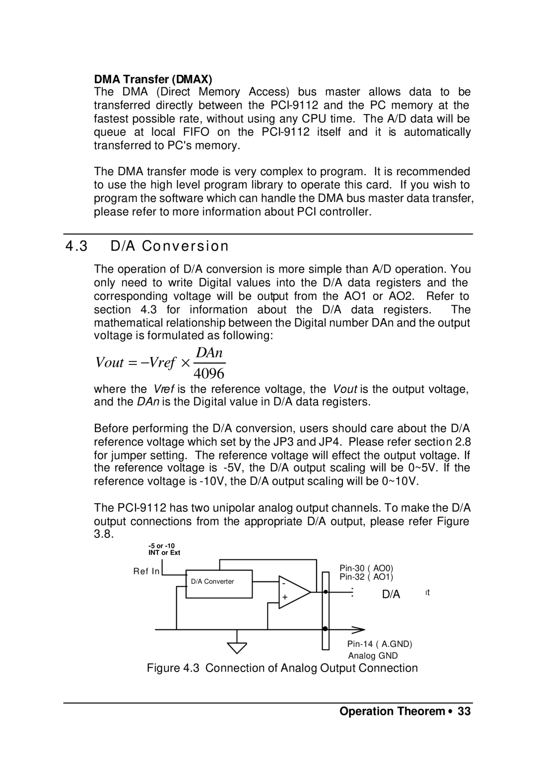
The operation of D/A conversion is more simple than A/D operation. You only need to write Digital values into the D/A data registers and the corresponding voltage will be output from the AO1 or AO2. Refer to
section 4.3 for information about the D/A data registers. The mathematical relationship between the Digital number DAn and the output voltage is formulated as following:
Vout = −Vref ×
DAn
4096
where the Vref is the reference voltage, the Vout is the output voltage, and the DAn is the Digital value in D/A data registers.
Before performing the D/A conversion, users should care about the D/A reference voltage which set by the JP3 and JP4. Please refer section 2.8 for jumper setting. The reference voltage will effect the output voltage. If the reference voltage is
The
Ref In |
| ||
| |||
D/A Converter | 餟 | ||
ToD/A Output | |||
| 儜 | ||
|
| ||
|
|
Analog GND