Developer’s Manual
537EX Chipset
Intel Confidential
Contents
Figures
Tables
Date Revision Description
Revision History
001 Initial release
Controllerless Modem Driver Overview
Introduction
Windows 95 and Windows
Tapi
V.90/V.92 and V.34 Data Modes
Unimodem
Intelsdb.VXD
Modem Connection Overview
DTE-to-DCE Data Rates for Each Mode
AT Commands Overview
DCE-to-DCE Data Rates for Each Mode
DCE-to-ISP Data Rates for V.90 Mode
Delayed Call
Sending Commands
DTE-Modem Data Rate Response Codes
Numeric Text
AT Escape Sequences
Command Function
Dial Modifier
Dialing digits
Command Function Default Range Reported By &Vn
Data Mode Command Summary
Intel Confidential
Intel Confidential
Intel Confidential
+ESA
+EB
+ESR
+ETBM
44/V.42/V.42 bis MNP Command Summary
Processes flow control characters and passes to local
Fax Class 1 Command Summary
Fax Identity Command Summary
Voice DTE→DCE Character Pairs
IS-101 Voice Command Summary
Response Hex Code Function
Voice DTE←DCE Character Pairs
Voice DTE →DCE Character Pairs
DEL
ESC
Dial Modifiers
Register Function Default Range Units Reported by &Vn
Register Summary
Ascii
Register Function Default Range Units
Modem Responses and Command Echo En, Vn, Xn, Wn, Qn
Using AT Commands to Access the S-Registers Sn?, Sn=x, ?
Modem Setup Host Modem Response Command
Data Reporting Wn Mapping
Disable Enable
DTE
Resets and then configures the modem to Nvram user profile
Establishing a Modem Connection A, D, DS = n, S0
AT Commands Product Information
Product Identification Information
Hanging Up Hn, S10, Zn, &D2
Online Command Mode Escape Codes, On
Modem-to-Modem Connection Data Rates
Intel Confidential
Modem-on-Hold Incoming Voice Call in Data Mode
Modem-on-Hold Initiating a Voice Call in Data Mode
Intel Confidential
Carrier Description
Supported Modulation Types
Local Analog Loopback AT&T1
Diagnostic Testing S18, &Tn
Local Modem or Test Modem
Local Analog Loopback With Self-Test AT&T8
Time-Independent Escape Sequence
AT Escape Sequences
Licensing Requirements for Hayes Escape Sequence
Example
Command Default Description
Data Mode Command Descriptions
Hayes* Escape Sequence
Host in either online or off-line command mode
Previously stored in the Nvram with the AT&Zn=x command
Echo disabled
Echo enabled
DTE
ATI2
Sn=x
Modem dials a telephone number touch tone dialing
Command
Numeric or verbose form
Numeric form
Subsequent commands to be ignored
Disconnecting
Resets the modem and recalls user profile
DCD or Rlsd signal
Active Profile
AT&V0
Stored Profile
Telephone Numbers
Command to see the stored telephone number
S-register configurations into the Nvram user profile ‘n’
Select profile
= 0-9 a B C D # * T P R W @
Indication Definition
Command Default
+EB
Nrzi encoding and decoding disabled
CRC generation and checking disabled
Secondary channel operation, and vice versa
12/V.34
+ETBM
+ESR
+GSN
+GMR
+IFC
+ILRR=m
+MA? will display a list of enabled alternative modulations
+MS command description
= carrier,carrier,…carrier
If +MS = ,0,, no alternative modulations will be available
BELL103
Carrier Description
BELL212
+MS=m See ‘m’
+PMHF
+PHSW=
Value Description
+PMHR
Enable Short Phase 1 and Short Phase
Conjunction with the +PSS command
Enable Short Phase
Disable short Phase 1 and Short Phase
Operating Modes
Mode Features
+ES Settings Answer Modem
44/V.42/V.42 bis and MNP Data Modem Command Descriptions
Resulting +ES Connection Types
+ES=1, 0 +ES=4, 4 +ES=3, 0 +ES=3, 2
\Bn
\Kn
Direction
+DR=m
+DS=m
Max string
+EFCS=m
3768
Decimal value and the format is as follows
Display messages when +ER =
+ER=m
+ER Lapm
Control during non-error control operation
Setting is ignored if origrqst=6
Non-error control operation
+ES=m
Fax Class 1 Commands
Fax Identity Commands
Fax Identity Command Descriptions
+FMFR?/+FMI
Value Modulation Speed bps
Mod Selection Table
Class 1 DTE-Generated Hdlc Frame Information AT+FTH=mod
30 Hdlc Frame Format
+FCLASS?
Fax Mode Command Descriptions
+FCLASS
+FRS=m
+FRH=m
+FTH=m
IS-101 Voice Mode AT Commands
Dtmf Detection Reporting
Voice Mode Command Descriptions
Relay Control
+FLO=m
+VDR=m See ‘m’
Enable report Function
Caller ID report Command Reserved Distinctive ringing All
Defaults = ‘C’, BB860980, BFE63883, BB863EE0
Event Description
+VEM=m See ‘m’
EX Value BIT Value Event
EIGHT-DIGIT HEX Code B B 8 6 3 E E
HEX Digit Location
128 Nominal transmit level
Local telephone, or speaker
+VIP
Label
Preassigned Voice I/O Labels
+VLS=m
Relay/Playback Control
Voice I/O Primitive Codes
Primitive Code Description
+VSD=m See ‘m’
+VRX
141 AD3 3-bit Adaptive differential pulse code modulation
+VSM=? command to obtain supported sampling rates
+VSM=m
Range 4800, 7200, 8000, and 11025 samples/second
Serial
Cml
Hard Disk
Compression
100 Default value 1 second
Factory default is ‘0’
100
Range 5-255 units of 0.01 seconds
+VTS=m None
Dual tones may be sent using the following format
Specified by +VTD=m
This sends a 500 ms period of silence
Command Default Description
Register Command Descriptions
S10
Escape sequences
Range Seconds Default 0 seconds
S16
S22 118
S21
S25
S30
Modem or when a ring signal is detected
Modem exits sleep mode whenever the host reads or writes to
Sleep mode is disabled by setting S33 to ‘0’
Inactive state when
Tag Description
Caller ID Tags for Formatted Reporting
Ring
Uart Emulation in Intelsdb.VxD
Uart Emulation in the Controllerless Modem
THR
Uart
RBR
Parallel Host Interface Uart Register Bit Assignments
Scratch Register SCR
Uart Register Definitions
Modem Status Register MSR
OE Overrun Error-Not supported
Bit Framing error
Line Status Register LSR
Stack
Procedure is as follows
IER Interrupt Enable register
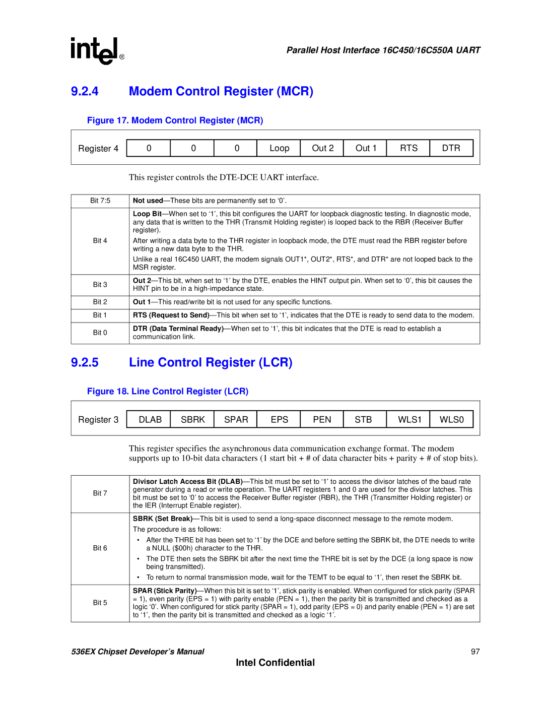
Modem Control Register MCR
Line Control Register LCR
Bit
Fifo Control Register FCR
Interrupt Control Functions
Interrupt Identity Register IIR
ID1 ID0
ID bit 2 for Fifo mode
Interrupt Enable Register IER
Transmitter Holding Register THR
Dlab =
Divisor Latch Registers DLM and DLL
Receiver Buffer Register RBR
Programmable Data Rates
Data Rate Divisor Number Divisor Latch Hex
Fifo Polled Mode Operation
Fifo Interrupt Mode Operation
16C550A Uart Fifo Operation
102
536EX Chipset Developer’s Manual 103