
D925XBC, D925XCV specifications
The Intel D925XBC and D925XCV are motherboards designed for Intel's LGA 775 socket, targeted primarily at the desktop market during the mid-2000s. These motherboards support Intel's innovative 800 MHz Front Side Bus and provide a robust platform for various computing applications, including gaming and multitasking.One of the standout features of the D925XBC and D925XCV is their compatibility with Intel's Pentium 4 and Pentium D dual-core processors. These processors deliver impressive performance, especially for users engaging in demanding tasks such as video editing and 3D rendering. The support for dual-channel DDR2 memory allows for increased bandwidth and improved overall system performance, accommodating up to 8 GB of memory in total.
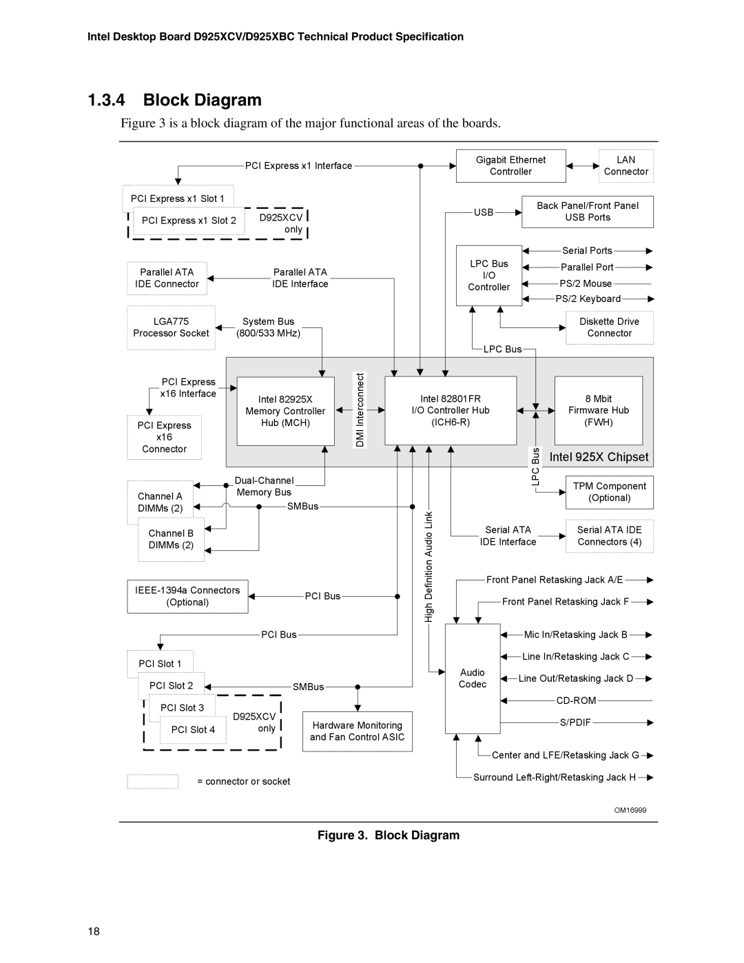
The motherboards are equipped with the Intel 925X chipset, which integrates advanced technologies. This chipset supports Intel's Enhanced Memory 64 Technology (EM64T), allowing for more efficient processing power and better resource management. The presence of the I/O Controller Hub (ICH6) also enhances connectivity options, including SATA 3.0 Gbps interfaces for faster data transfer rates and improved storage capabilities.
Regarding expansion and connectivity, both motherboards feature multiple PCI Express slots along with PCI slots, allowing users to customize their systems according to their needs. This expandability is essential for gamers and professionals looking to add advanced graphics cards and other peripherals. Additionally, these boards come with integrated audio, ensuring satisfactory sound quality without the need for additional sound cards.
The D925XBC and D925XCV motherboards also include integrated Ethernet controllers, supporting fast network connectivity essential for gaming and high-speed internet access. With multiple USB ports available, users can connect a wide variety of devices easily, enhancing the flexibility of their setups.
In terms of form factor, both boards follow the ATX layout, providing compatibility with a broad range of computer cases. This ensures ease of installation and upgrades while promoting good airflow and optimal thermal management for the components installed.
Overall, the Intel D925XBC and D925XCV motherboards integrate essential features and technologies that provide a solid foundation for desktop computing during their time. With strong processing capabilities, expandability, and good connectivity options, these boards were well-received by users looking for reliable performance and versatility in their systems.