LXD9785 PQFP Demo Board with FPGA for SS-SMII (Fiber)-to-MII Conversion

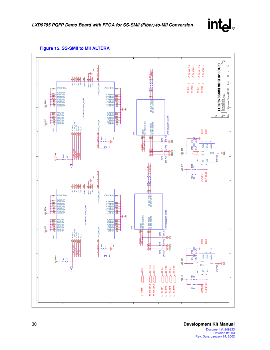
Figure 15. SS-SMII to MII ALTERA

4

3

2

1

E

D

C

B


GND

FPGA I


SYNC


75

76

129

186

180


185


25

26

130


151


CKLK_VCC


TMS TCK

TDI TRST

TDO

nCEO

MSEL0 MSEL1

nCE

FPGA OUT


CKLK_GND


125


128


_


VCCINT9


SYNC


182


GNDINT8


156

VCCINT8


183


126

VCCINT7


GNDINT7

143


105

VCCINT6


EP20K100QC208-1 SS SMII


GNDINT6

127


79

VCCINT5


GNDINT5

118


52

VCCINT4


GNDINT4

78


28

VCCINT3


GNDINT3

39


23

VCCINT2


GNDINT2

24


FPGAVCC


1

VCCINT1


GNDINT1

16


VCCIO8


GNDIO8


208

VCCIO7


GNDIO7

199


189


169


172

VCCIO6


GNDIO6

149


136

VCCIO5


GNDIO5

114


86

VCCIO4


GNDIO4

95


80

VCCIO3


GNDIO3

64


53

VCCIO2


GNDIO2

43


VCCEXT


8

VCCIO1


nCONFIG CONFDONE

nSTATUS DATA0


SYNCFPGAIN


GNDIO1

10


U31E


DCLK


29

83

82

133

132


73


FPGA O


R565


1K


GND


FPGA


R549

1K

CONF DONE1

nSTATUS1

DATA1

DCLK1


SYNC_


X51


VCC


X35


GND

SYNC FPGA O


75

76

129

186

180


185


25

26

130


151


CKLK_VCC


TMS TCK

TDI TRST

TDO

nCEO

MSEL0 MSEL1

nCE

FPGA OUT


CKLK_GND


125


128


_


VCCINT9


SYNC


182


GNDINT8


VCCINT8


156


183


VCCINT7


GNDINT7


126


143


VCCINT6


EP20K100QC208-1 SS SMII


GNDINT6


105


127


VCCINT5


GNDINT5


79


118


VCCINT4


GNDINT4


52


78


VCCINT3


GNDINT3


28


39


VCCINT2


GNDINT2


23


24


VCCINT1


GNDINT1


FPGAVCC

1


16


VCCIO8


GNDIO8


208

VCCIO7


GNDIO7

199


189


169


VCCIO6


GNDIO6


172


149


VCCIO5


GNDIO5


136


114


VCCIO4


GNDIO4


86


95


VCCIO3


GNDIO3


80


64


VCCIO2


GNDIO2


53


43


VCCIO1


GNDIO1


VCCEXT

8


nCONFIG CONFDONE

nSTATUS DATA0


SYNCFPGAIN


10


U30E


DCLK


GND

U31F

GND

U30F


TX CLK1


TX SYNC1


50 1%


50 1%


R731


R567


112


147


SS SMII TXCLK

SS SMII TXSYNC


nRESET

CLK(125REF MHz)


SMIISSRXCLK

SMIISSRXSYNC


-1 SS SMII


CAPPAD

EP20K100QC208


188

27


131

184


C345


nRESET

REF CLK 3


GNDGND GND


RX CLK1


RX SYNC1


C344


CAPPAD


C343


PAD


TX CLK0


TX SYNC0


CAP


50 1%


50 1%


R562


R563


112


147


SS SMII TXCLK

SS SMII TXSYNC


nRESET CLK(125REF MHz)

SMIISSRXCLK

SMIISSRXSYNC


-1 SS SMII


CAPPAD

EP20K100QC208


188

27


131

184


C342


CLK2


GND


TX CLK0 3,16

TX SYNC0 3,16

TX CLK1 3,16

TX SYNC1 3,16


DV BOARD


TX SYNC0


TX SYNC1


SS/SMII MII FX

TX CLK0


TX CLK1


LXD9785


Title


DATA1

DCLK1

C183

0.01uF

1

2

6

EXT

C182

0.1uF

DATA

DCLK

nCASC


_


8

VCC


VCC


VCC


GND


5


7


EPC1PC8


U33

OE

nCS


EXT

R551

1K

3

4


VCC


R550

1K

nSTATUS1

CONF DONE1


Rev

A2


18


of


13


Sheet

Document Number

SS-SMII TO MII ALTERA

Wednesday, February 21, 2001


Date:

Size

B

GND

E

D

C

B


29

83

82

133

132

73


CONF DONE0


nSTATUS0


DATA0


DCLK0


SYNC FPGA I


R564


1K


GND


FPGA


R27

1K


X50


VCC


nRESET REF_

RX CLK

RX SYNC


C341


CAPPAD


GNDGND


C340


PAD


CAP


VCC_EXT

C154 C155

0.01uF

0.1uF

8

DATA0

DCLK0


1


2


6


DATA

DCLK

nCASC

VCC


GND

5

GND

X34

nRESET

REF_CLK_2

REF_CLK_3

RX_CLK

RX_SYNC

RX_CLK1

RX_SYNC1

7 U6

VCC


OE

nCS

EPC1PC8

A

3 nRESET

14 REF_CLK_2

14 REF_CLK_3

3,16 RX_CLK

3,16 RX_SYNC

3,16 RX_CLK1

3,16 RX_SYNC1

EXT

R29

1K

3

4

VCC


R28

1K

nSTATUS0

CONF DONE0

A

4

3

2

1

30

Development Kit Manual

Document #: 249323 Revision #: 003 Rev. Date: January 24, 2002

Page 30
Image 30
Intel 249323-003, Demo Board with FPGA for SS-SMII (Fiber)-to-MII Conversion manual SS-SMII to MII Altera

249323-003, Demo Board with FPGA for SS-SMII (Fiber)-to-MII Conversion specifications

The Intel 249323-003 demo board is an advanced platform designed for SS-SMII (Synchronous Serial - Synchronous Media Independent Interface) to MII (Media Independent Interface) conversion, utilizing FPGA technology. This demo board serves as a pivotal tool for developers and engineers in the field, facilitating the evaluation and testing of high-speed networking applications, particularly those involving fiber-optic communication.

At its core, the Intel 249323-003 is equipped with a robust FPGA that is capable of handling complex data processing tasks with high efficiency. The FPGA architecture allows for flexible configuration, enabling users to customize the interface as per their specific application requirements. This adaptability is crucial in developing solutions for various networking protocols, ensuring seamless integration across different mediums.

One of the standout features of the demo board is its support for fiber-optic connections, which are essential for high-speed data transmission over long distances. The board includes interfaces that allow for the connection of fiber transceivers, thereby facilitating faster communication speeds and improved bandwidth efficiency. This capability is particularly beneficial for applications in data centers, telecommunications, and other high-bandwidth scenarios.

Additionally, the Intel 249323-003 demo board showcases low latency performance, a critical characteristic for real-time applications. This feature is achieved through sophisticated design and optimization techniques that ensure quick data processing. The board also supports various data rates, making it versatile enough for different use cases.

Another important aspect is the board’s power consumption efficiency. By implementing advanced power management techniques, the Intel 249323-003 minimizes energy usage while maximizing performance, making it a cost-effective solution for developers looking to create sustainable applications.

In terms of connectivity, the demo board offers multiple I/O options, facilitating interaction with other devices and systems. This eases the development process, allowing engineers to prototype and test their designs rapidly.

In conclusion, the Intel 249323-003 demo board is a sophisticated and versatile platform for SS-SMII to MII conversion. With its powerful FPGA, support for fiber-optic interfaces, low latency, and efficient power management, it stands out as a vital resource for developers working on high-speed networking solutions. Whether for prototyping or extensive testing, this demo board equips engineers with the tools necessary to innovate and elevate their networking projects to new heights.