SSI
ERP2U Power Supply Design Guide, V1.0
6.11 Timing Requirements
STATUS
Required
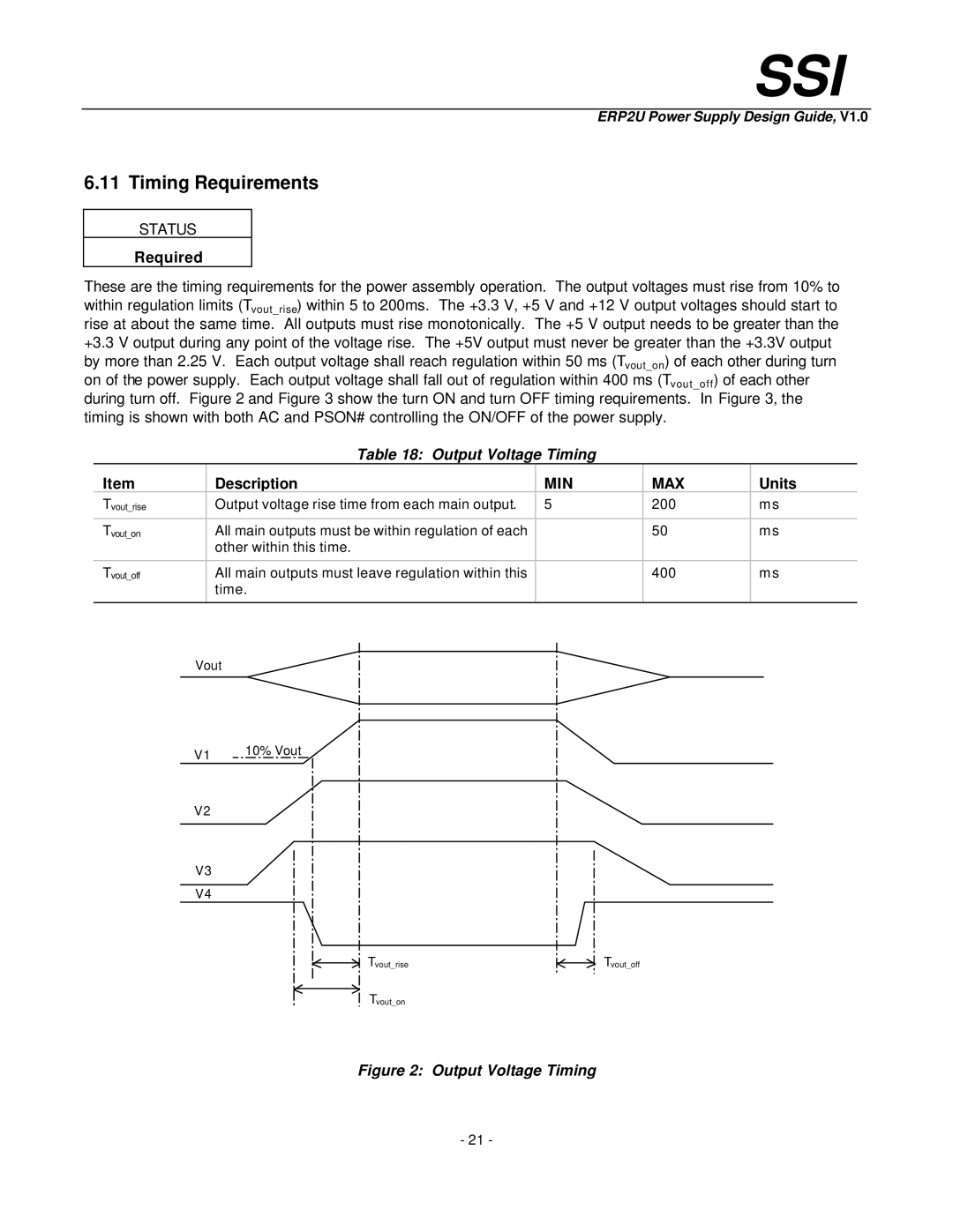
These are the timing requirements for the power assembly operation. The output voltages must rise from 10% to within regulation limits (Tvout_rise) within 5 to 200ms. The +3.3 V, +5 V and +12 V output voltages should start to rise at about the same time. All outputs must rise monotonically. The +5 V output needs to be greater than the +3.3 V output during any point of the voltage rise. The +5V output must never be greater than the +3.3V output by more than 2.25 V. Each output voltage shall reach regulation within 50 ms (Tvout_on) of each other during turn on of the power supply. Each output voltage shall fall out of regulation within 400 ms (Tvout_off) of each other during turn off. Figure 2 and Figure 3 show the turn ON and turn OFF timing requirements. In Figure 3, the timing is shown with both AC and PSON# controlling the ON/OFF of the power supply.
Table 18: Output Voltage Timing
Item |
|
| Description | MIN |
|
| MAX | Units | ||||||||||||||
Tvout_rise |
|
| Output voltage rise time from each main output. | 5 |
|
|
|
|
|
| 200 | ms | ||||||||||
|
|
|
|
|
|
|
|
|
|
|
|
|
|
|
|
|
|
|
|
|
|
|
Tvout_on |
|
| All main outputs must be within regulation of each |
|
|
|
|
|
|
| 50 |
| ms | |||||||||
|
|
| other within this time. |
|
|
|
|
|
|
|
|
|
|
|
| |||||||
|
|
|
|
|
|
|
|
|
|
|
|
|
|
|
|
|
|
|
|
|
|
|
Tvout_off |
|
| All main outputs must leave regulation within this |
|
|
|
|
|
|
| 400 | ms | ||||||||||
|
|
| time. |
|
|
|
|
|
|
|
|
|
|
|
| |||||||
|
|
|
|
|
|
|
|
|
|
|
|
|
|
|
|
|
|
|
|
|
| |
|
|
|
|
|
|
|
|
|
|
|
|
|
|
|
|
|
|
|
| |||
| Vout |
|
|
|
|
|
|
|
|
|
|
|
| |||||||||
|
|
|
|
|
|
|
|
|
|
|
|
|
|
|
|
|
|
|
|
|
|
|
|
|
|
|
|
|
|
|
|
|
|
|
|
|
|
|
|
|
|
|
|
| |
|
|
|
|
|
|
|
|
|
|
|
|
|
|
|
|
|
|
|
|
| ||
| V1 | 10% Vout |
|
|
|
|
|
|
|
|
|
|
|
| ||||||||
|
|
|
|
|
|
|
|
|
|
|
|
|
|
|
|
|
|
|
|
| ||
| V2 |
|
|
|
|
|
|
|
|
|
|
|
|
|
|
|
|
|
|
|
| |
|
|
|
|
|
|
|
|
|
|
|
|
|
|
|
|
|
|
|
|
| ||
|
|
|
|
|
|
|
|
|
|
|
|
|
|
|
|
|
|
|
|
|
| |
| V3 |
|
|
|
|
|
|
|
|
|
|
|
|
|
|
|
|
|
|
|
| |
|
|
|
|
|
|
|
|
|
|
|
|
|
|
|
|
|
|
|
|
| ||
|
|
|
|
|
|
|
|
|
|
|
|
|
|
|
|
|
|
|
|
|
| |
| V4 |
|
|
|
|
|
|
|
|
|
|
|
|
|
|
|
|
|
|
|
| |
|
|
|
|
|
|
|
|
|
|
|
|
|
|
|
|
|
|
|
|
|
| |
|
|
|
|
|
|
|
|
|
| Tvout_rise |
|
|
|
|
| Tvout_off |
|
|
| |||
|
|
|
|
|
|
|
|
|
|
|
|
|
|
|
|
|
| |||||
|
|
|
|
|
|
|
|
|
| Tvout_on |
|
|
|
|
|
|
|
|
|
|
|
|
|
|
|
|
|
|
|
|
|
|
|
|
|
|
|
|
|
|
|
|
|
| |
Figure 2: Output Voltage Timing
- 21 -
