
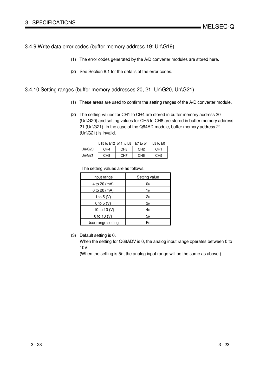
Q68ADV, Q68ADI, Q64AD specifications
Mitsubishi Electronics, a renowned leader in automation technology, has developed advanced analog input modules that play a crucial role in numerous industrial applications. Among them, the Q64AD, Q68ADI, and Q68ADV models stand out with their impressive features and capabilities tailored for precise data acquisition and control.The Q64AD module is designed for high-performance analog signal processing. It offers up to 16 channels of differential input, making it suitable for applications requiring multiple sensor readings simultaneously. The resolution of 16 bits enables accurate data capture, ensuring that subtle variations in process variables, such as temperature or pressure, are detectable. One of its key advantages is the high-speed sampling capability, allowing data collection at rates of up to 100 milliseconds per channel, essential for real-time monitoring in fast-paced environments.
In contrast, the Q68ADI model enhances the versatility of the analog input system. It includes built-in isolators, providing additional protection against noise and interference commonly found in industrial settings. This isolation feature improves the reliability of sensor readings, especially in harsh environments where electrical noise can impact performance. Furthermore, the Q68ADI supports both voltage and current input types, making it adaptable to various sensor configurations, such as thermocouples and RTDs, expanding its usability across different applications.
The Q68ADV module takes versatility a step further by integrating advanced diagnostic features. This model offers a range of additional functions, including built-in fault detection and self-diagnosis capabilities that identify issues before they escalate into significant problems. It also features temperature compensation and linearization algorithms, which enhance the accuracy of reading from thermocouples and other temperature sensors. The Q68ADV module is ideal for applications demanding high reliability and stringent performance standards, making it indispensable in industries like pharmaceuticals and food processing.
All three models are designed to seamlessly integrate with Mitsubishi's PLC systems, ensuring smooth communication and data exchange. They support various protocols, making them compatible with a wide range of devices and systems. Collectively, the Q64AD, Q68ADI, and Q68ADV modules exemplify Mitsubishi Electronics' commitment to delivering high-quality, reliable, and innovative solutions in industrial automation, empowering businesses to achieve greater efficiency and operational excellence.