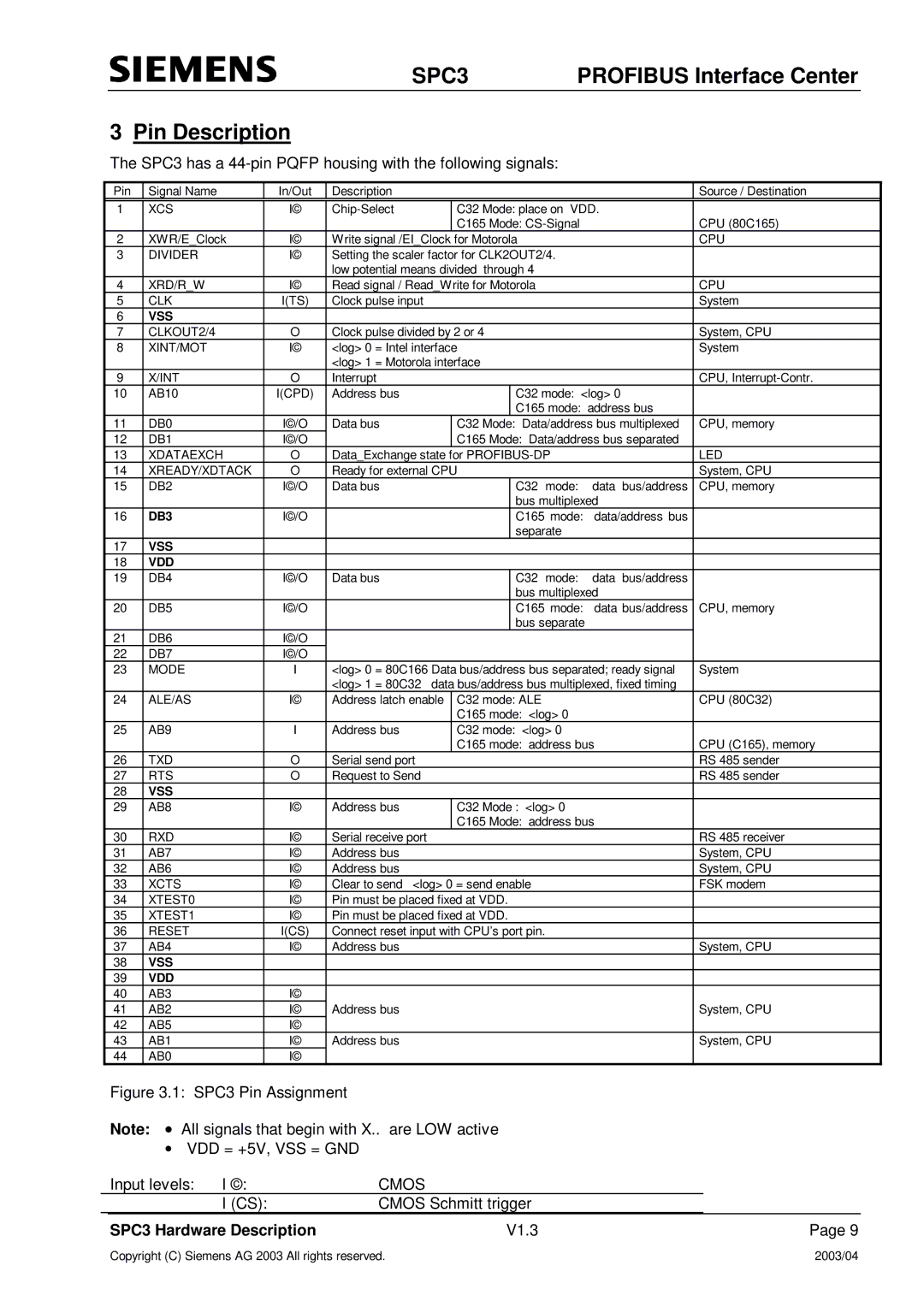
SPC3 specifications
Siemens SPC3 is a state-of-the-art solution designed to enhance industrial automation, providing businesses with a robust platform for managing complex processes efficiently. This device epitomizes Siemens' commitment to innovation, blending cutting-edge technology with user-friendly features to deliver optimized performance across various applications.One of the standout features of the Siemens SPC3 is its advanced processing capabilities. Equipped with high-performance processors, it can handle various tasks simultaneously, ensuring seamless operation even in demanding environments. This performance is complemented by enhanced memory capacity, which allows for increased data handling and improved execution speed, crucial for real-time monitoring and control applications.
The Siemens SPC3 also integrates a modular design, enabling flexibility and scalability. This characteristic allows users to customize their systems according to specific operational needs, adding or removing components as required. This adaptability is particularly beneficial for businesses that aim to scale their operations without incurring the substantial costs associated with overhauling existing systems.
Furthermore, the SPC3 employs the latest communication technologies, ensuring interoperability with various devices and systems. It supports industry-standard protocols, facilitating efficient data exchange between components. This connectivity is vital for establishing smart factories and enhancing overall productivity by creating a unified ecosystem.
Another significant aspect of the Siemens SPC3 is its focus on security. As cyber threats in industrial settings become increasingly sophisticated, Siemens prioritizes safeguarding user data and system integrity. The SPC3 incorporates advanced security features, including encryption and access control measures, to protect against unauthorized access and ensure data confidentiality.
Siemens has also emphasized ease of use in the SPC3. The interface is designed to be intuitive, allowing operators to navigate and configure the system effortlessly. Coupled with comprehensive software tools, users are empowered to implement changes swiftly while minimizing downtime.
In terms of energy efficiency, the SPC3 incorporates technologies that allow for optimized energy consumption, aligning with sustainability goals prevalent in today’s industries. By reducing energy waste, businesses not only lower operational costs but also contribute to environmental conservation.
In summary, Siemens SPC3 represents a significant advancement in industrial automation technology. Its high-performance processing, modular adaptability, advanced communication capabilities, robust security measures, and user-friendly design make it an ideal choice for businesses striving for efficiency and innovation in their operations. The SPC3 is more than just a control device; it is a comprehensive solution that meets the evolving demands of modern industries.

