SWRA004A
High-Band LO Buffer Amplifier Output
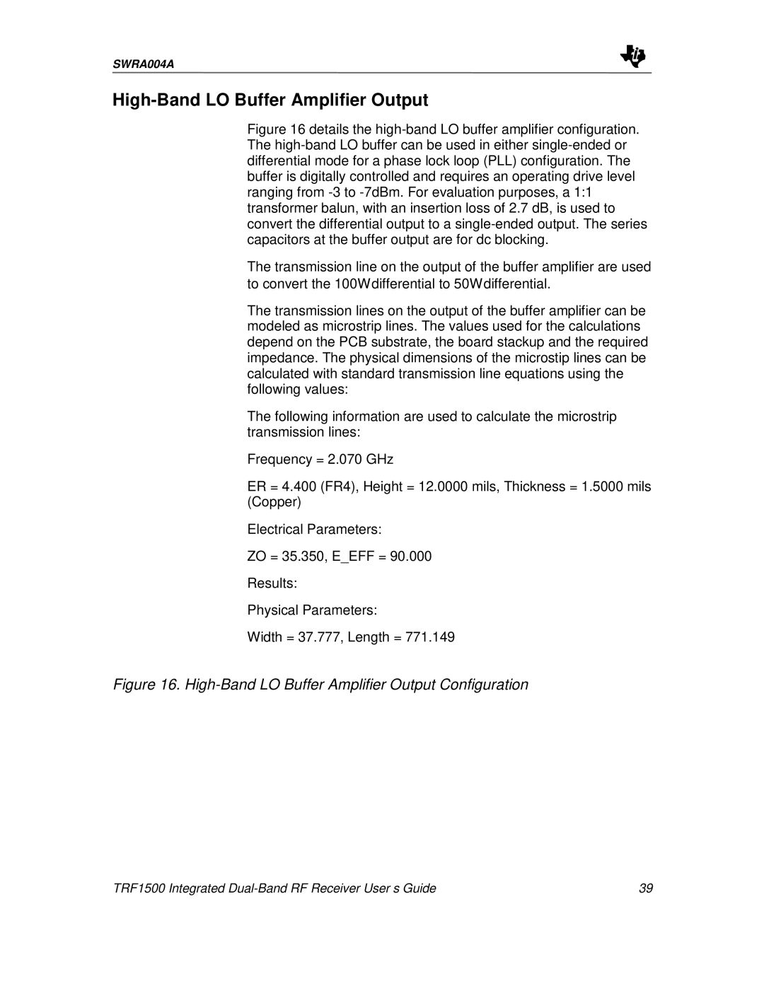
Figure 16 details the high-band LO buffer amplifier configuration. The high-band LO buffer can be used in either single-ended or differential mode for a phase lock loop (PLL) configuration. The buffer is digitally controlled and requires an operating drive level ranging from -3 to -7dBm. For evaluation purposes, a 1:1 transformer balun, with an insertion loss of 2.7 dB, is used to convert the differential output to a single-ended output. The series capacitors at the buffer output are for dc blocking.
The transmission line on the output of the buffer amplifier are used to convert the 100Ω differential to 50Ω differential.
The transmission lines on the output of the buffer amplifier can be modeled as microstrip lines. The values used for the calculations depend on the PCB substrate, the board stackup and the required impedance. The physical dimensions of the microstip lines can be calculated with standard transmission line equations using the following values:
The following information are used to calculate the microstrip transmission lines:
Frequency = 2.070 GHz
ER = 4.400 (FR4), Height = 12.0000 mils, Thickness = 1.5000 mils (Copper)
Electrical Parameters:
ZO = 35.350, E_EFF = 90.000
Results:
Physical Parameters:
Width = 37.777, Length = 771.149
Figure 16. High-Band LO Buffer Amplifier Output Configuration
TRF1500 Integrated | 39 |