1. Product Specification (continued)
ACER G24
3
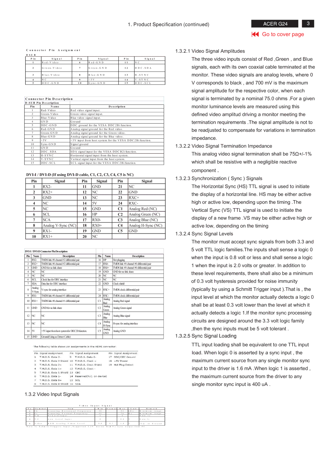
C o n n e c t o r P i n A s s i g n m e n t
D S U B
P i n | S i g n a l | P i n | S i g n a l | P i n | S i g n a l |
1 | R e d - V i d e o | 6 | R e d - G N D | 1 1 | N C |
2 | G r e e n - V i d e o | 7 | G r e e n - G N D | 1 2 | D D C - S D A |
|
|
|
|
|
|
3 | B l u e - V i d e o | 8 | B l u e - G N D | 1 3 | H - S Y N C |
|
|
|
|
|
|
4 | N C | 9 | + 5 V | 1 4 | V - S Y N C |
5 | D D C - G N D | 1 0 | S y n c - G N D | 1 5 | D D C - S C L |
C o n n e c to r P in D e s c rip tio n
D -S U B P in D e s c riptio n
P in | N a m e | D e s c riptio n |
1 | R e d - V id e o | R e d vid e o signa l inp ut. |
2 | G re e n- V id e o | G re e n vid e o signa l inp ut. |
3 | B lue - V id e o | B lue vid e o signa l inp ut. |
4 | G N D | G ro und |
5 | D D C - G N D | D D C gro und fo r the V E S A D D C 2 B i func tio n. |
6 | R e d - G N D | A na lo g signa l gro und fo r the R e d vid e o . |
7 | G re e n- G N D | A na lo g signa l gro und fo r the G re e n vid e o . |
8 | B lue - G N D | A na lo g signa l gro und fo r the B lue vid e o . |
9 | + 5 V | + 5 V inp ut fro m ho st syste m fo r the V E S A D D C 2 B i func tio n. |
1 0 | S ync - G N D | S igna l gro und |
1 1 | G N D | G ro und |
1 2 | D D C _ S D A | S D A signa l inp ut fo r the V E S A D D C B 2 i func tio n. |
1 3 | H - S Y N C | H o rizo nta l signa l inp ut fro m the ho st syste m. |
1 4 | V - S Y N C | V e rtic a l signa l inp ut fro m the ho st syste m. |
1 5 | D D C - S C L | S C L signa l inp ut fo r the V E S A D D C 2 B i func tio n. |
|
| Pin | Signal |
| Pin |
| Signal | Pin | Signal | ||
|
| 1 | RX2- |
| 11 | GND |
| 21 | NC | ||
|
| 2 | RX2+ |
| 12 | NC |
| 22 | GND | ||
|
| 3 | GND |
| 13 | NC |
| 23 | RXC+ | ||
|
| 4 | NC |
| 14 | 5V |
| 24 | RXC- | ||
|
| 5 | NC |
| 15 | GND |
| C1 | Analog Red (NC) | ||
|
| 6 | SCL |
| 16 | HP |
| C2 | Analog Green (NC) | ||
|
| 7 | SCA |
| 17 | RX0- |
| C3 | Analog Blue (NC) | ||
|
| 8 | Analog |
| 18 | RX0+ |
| C4 | Analog | ||
|
| 9 | RX1- |
| 19 | GND |
| C5 | GND | ||
|
| 10 | RX1+ |
| 20 | NC |
|
|
|
| |
|
|
|
|
|
|
|
|
|
|
| |
|
|
|
|
|
|
|
|
| |||
| Pin | Name | Description |
|
| Pin | Name |
| Description |
| |
| 1 | RX2- | TMDS link #0 channel#2 differentialpair |
|
| 16 | HP | Hot plugging |
|
| |
| 2 | RX2+ | TMDS link #0 channel#2 differentialpair |
|
| 17 | RX0- | TMDS link #0 channel#0 differentialpair |
| ||
| 3 | GND | GNDfor no link share |
|
| 18 | RX0+ | TMDS link #0 channel#0 differentialpair |
| ||
| 4 | NC | NC |
|
| 19 | GND | GNDfor no link share |
| ||
| 5 | NC | NC |
|
| 20 | NC | NC |
|
| |
| 6 | SCL | Clock line for DDC interface |
|
| 21 | NC | NC |
|
| |
| 7 | SDA | Data line for DDC interface |
|
| 22 | GND | Clock shield |
|
| |
| 8 | Analog |
|
| 23 | RXC+ | TMDS clock differentialpair |
| |||
|
|
|
|
|
|
|
|
|
|
| |
| 9 | RX1- | TMDS link #0 channel#1 differentialpair |
|
| 24 | RXC- | TMDS clock differentialpair |
| ||
| 10 | RX1+ | TMDS link #0 channel#1 differentialpair |
|
| C1 | Analog | AnalogRed signal |
| ||
|
|
|
|
|
|
|
| Red |
|
|
|
| 11 | GND | GNDfor no link share |
|
| C2 | Analog | AnalogGreensignal |
| ||
|
|
|
|
|
|
|
| Green |
|
|
|
| 12 | NC | NC |
|
| C3 | Analog | AnalogBlue signal |
| ||
|
|
| Blue |
| |||||||
| 13 | NC | NC |
|
| C4 | Analog |
| |||
|
|
|
|
|
|
|
|
|
|
| |
| 14 | 5V | +5Vinput fromhost systemfor DDC2Bfunction. |
| C5 | Analog | AnalogGND |
|
| ||
|
|
|
|
|
|
|
| GND |
|
|
|
| 15 | GND | Ground(Usingas Detect Cable) |
|
|
|
|
|
|
| |
Go to cover page
1.3.2.1Video Signal Amplitudes
The three video inputs consist of Red ,Green , and Blue signals, each with its own coaxial cable terminated at the monitor. These video signals are analog levels, where 0 V corresponds to black , and 700 mV is the maximum signal amplitude for the respective color, when each signal is terminated by a nominal 75.0 ohms .For a given monitor luminance levels are measured using this defined video amplitud driving a monitor meeting the termination requirements .The signal amplitude is not to be readjusted to compensate for variations in termination impedance.
1.3.2.2Video Signal Termination Impedance
This analog video signal termination shall be
1.3.2.3Synchronization ( Sync ) Signals
The Horizontal Sync (HS) TTL signal is used to initiate the display of a horizontal line. HS may be either active high or active low, depending upon the timing .The Vertical Sync (VS) TTL signal is used to initiate the display of a new frame .VS may be either active high or active low, depending on the timing
1.3.2.4Sync Signal Levels
The monitor must accept sync signals from both 3.3 and 5 volt TTL logic families.The inputs shall sense a logic 0 when the input is 0.8 volt or less and shall sense a logic 1 when the input is 2.0 volts or greater. In addition to these level requirements, there shall also be a minimum of 0.3 volt hysteresis provided for noise immunity (typically by using a Schmitt Trigger input ).That is , the input level at which the monitor actually detects a logic 0 shall be at least 0.3 volt lower than the level at which it actually detects a logic 1.If the monitor sync processing circuits are designed around the 3.3 volt logic family ,then the sync inputs must be 5 volt tolerant .
1.3.2.5Sync Signal Loading
1.3.2 Video Input Signals
|
|
|
| V i d e o | I n p u t | S i g n a l |
|
|
|
|
|
| ||
|
|
|
|
|
|
|
|
|
|
|
| |||
N o . | S y m b o l |
|
| I t e m |
| M i n | N o r m a l | M a x |
| U n i t | R e m a r k | |||
1 | F h | S c a n n i n g | H o r i z o n t a l F r e q u e n c y | 3 | 0 |
| 9 4 |
| k H z | M i n i m u m | r a n g e | |||
2 | F v | S c a n n i n g | V e r t i c a l F r e q u e n c y |
| 5 | 5 |
| 7 6 |
| H z | M i n i m u m | r a n g e | ||
3 | V i h | H i L e v e l I n p u t |
|
| 2 |
|
| 5 |
|
| N o t e 1 ) |
| ||
4 | V i l | L o w | L e v e l I n p u t |
|
| 0 |
| 0 | . 8 |
| V | N o t e 1 ) |
| |
|
|
|
|
|
|
|
|
|
|
|
|
| ||
5 | V i d e o | R G B | A n a l o g V i d e o L e v e l |
| 0 . 0 | 0 . 7 | 1 | . 0 |
| V | 7 5 Ω t o | G r o u n d | ||
|
|
|
|
|
|
|
|
|
|
|
| |||
N o t e | 1 ) S c h m i t t - T r i g g e r s | I n p u t , S u p p o r t e d | 3 . 3 V | d e v i c e | H ( & V ) | s y n c | o u t p u t f r o m | P C . |
| |||||
TTL input loading shall be equivalent to one TTL input load. When logic 0 is asserted by a sync input , the maximum current source from any single monitor sync input to the driver is 1.6 mA .When logic 1 is asserted , the maximum current source from the driver to any single monitor sync input is 400 uA .