Using the STK594 Top Module
2.3Programming the AT94K Devices
The FPSLIC configuration process involves configuring the FPGA, the AVR® program code and the FPSLIC data memory. This configuration requires a single bitstream that configures the FPGA, the embedded AVR Program SRAM and the FPSLIC Data SRAM. The combined bitstream is automatically generated by the Bitstream Generator, a System Designer software utility.
After a reset and the internal clearing of the configuration data, the FPSLIC device self- initiates configuration. The Master mode uses an internal oscillator to provide the Con- figuration Clock (CCLK) for clocking the external EEPROM (configurator), which contains the configuration data. After
Note: The AT94K devices also support
Note: The AT94K devices also support Cache Logic® Configuration. For more infor- mation on this topic, refer to the “Cache Logic Configuration” application note available on the Atmel web site.
For more details on programming procedures, refer to Section 4.10.
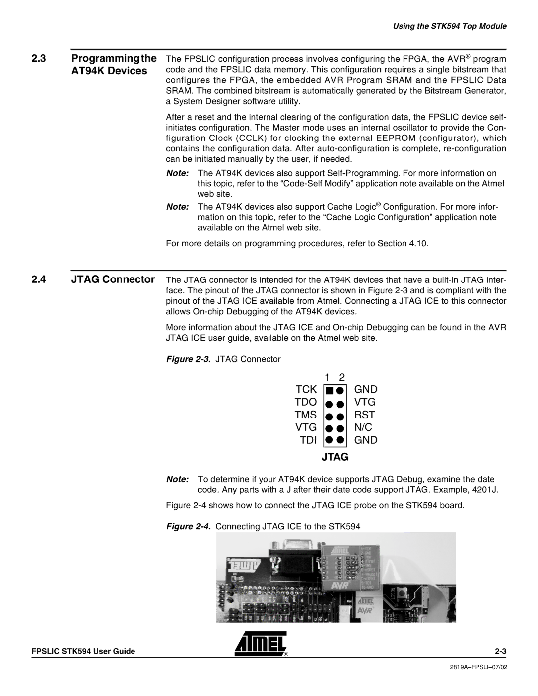
2.4JTAG Connector The JTAG connector is intended for the AT94K devices that have a
More information about the JTAG ICE and
JTAG ICE user guide, available on the Atmel web site.
Figure 2-3. JTAG Connector
1 2 TCK ![]()
![]() TDO
TDO ![]()
![]() TMS
TMS ![]()
![]() VTG
VTG ![]()
![]()
TDI
GND VTG RST N/C
GND
JTAG
Note: To determine if your AT94K device supports JTAG Debug, examine the date code. Any parts with a J after their date code support JTAG. Example, 4201J.
Figure 2-4 shows how to connect the JTAG ICE probe on the STK594 board.
Figure 2-4. Connecting JTAG ICE to the STK594
FPSLIC STK594 User Guide