Connect Tech
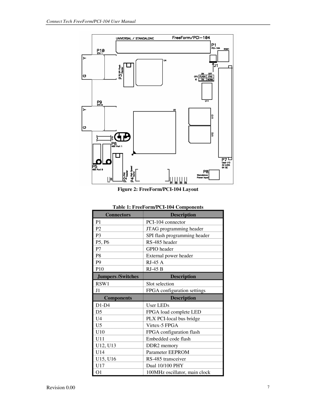
Figure 2: FreeForm/PCI-104 Layout
Table 1: FreeForm/PCI-104 Components
| Connectors | Description |
|
| P1 |
| |
| P2 | JTAG programming header |
|
| P3 | SPI flash programming header |
|
| P5, P6 |
| |
| P7 | GPIO header |
|
| P8 | External power header |
|
| P9 |
| |
| P10 |
|
| Jumpers /Switches | Description |
|
| RSW1 | Slot selection |
|
| J1 | FPGA configuration settings |
|
| Components | Description |
|
| User LEDs |
| |
| D5 | FPGA load complete LED |
|
| U4 | PLX |
|
| U5 |
| |
| U10 | FPGA configuration flash |
|
| U11 | Embedded code flash |
|
| U12, U13 | DDR2 memory |
|
| U14 | Parameter EEPROM |
|
| U15, U16 |
| |
| U17 | Dual 10/100 PHY |
|
| O1 | 100MHz oscillator, main clock |
|
Revision 0.00 | 7 |