Connect Tech
Reference Design
The
Functionality
oLocal bus interface driven at 50MHz o Slave access to:
o BAR2: 16x32 bit control registers , 16x32 bit user memory
o BAR3: SPI flash programming interface
o Master access to same 16x32 user memory as located in BAR2. Transfer controlled through slave accessible registers.
o Local bus master configuration of bridge (happens automatically with reset). o
o LED control through registers.
Memory Map
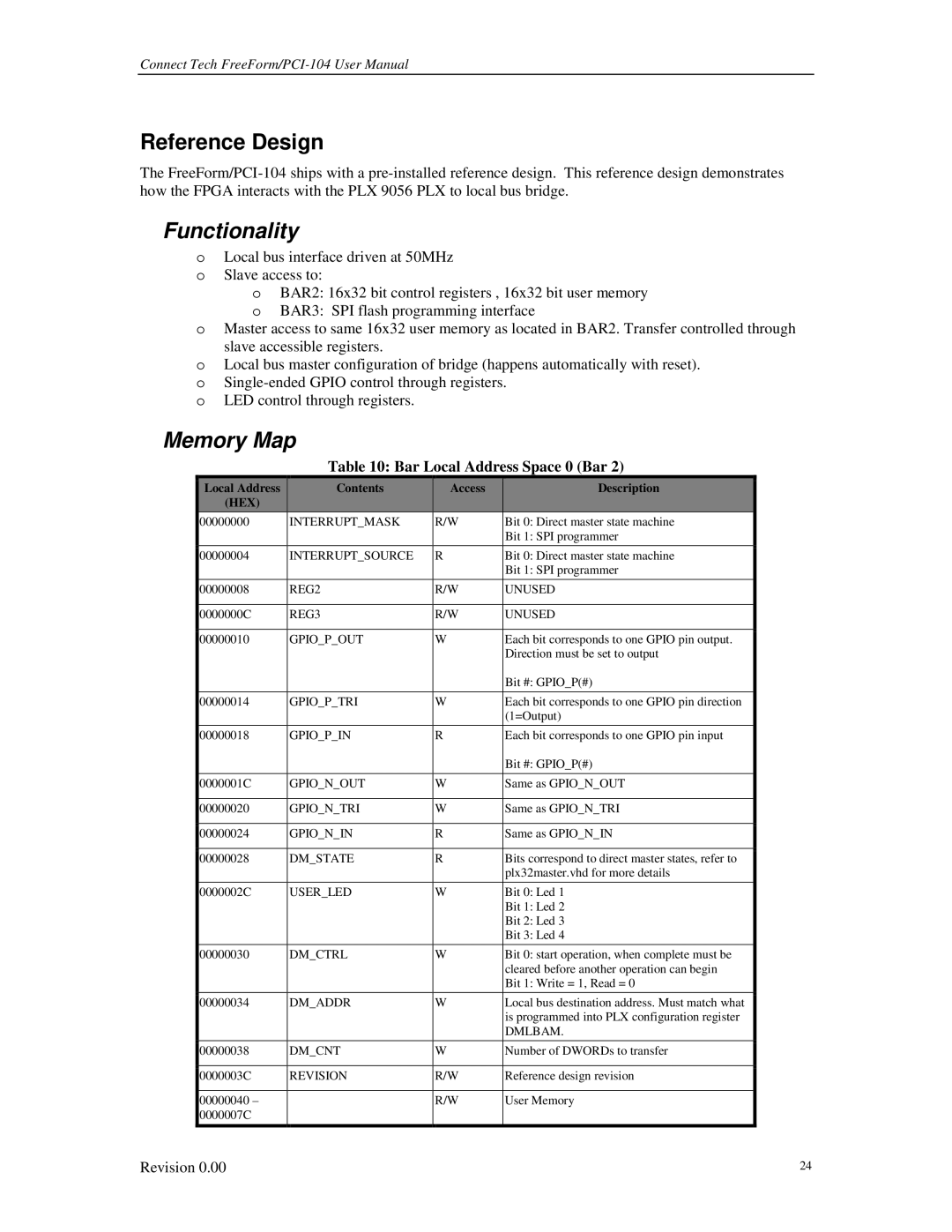
Table 10: Bar Local Address Space 0 (Bar 2)
Local Address | Contents | Access | Description |
(HEX) |
|
|
|
00000000 | INTERRUPT_MASK | R/W | Bit 0: Direct master state machine |
|
|
| Bit 1: SPI programmer |
|
|
|
|
00000004 | INTERRUPT_SOURCE | R | Bit 0: Direct master state machine |
|
|
| Bit 1: SPI programmer |
|
|
|
|
00000008 | REG2 | R/W | UNUSED |
|
|
|
|
0000000C | REG3 | R/W | UNUSED |
|
|
|
|
00000010 | GPIO_P_OUT | W | Each bit corresponds to one GPIO pin output. |
|
|
| Direction must be set to output |
|
|
| Bit #: GPIO_P(#) |
|
|
|
|
00000014 | GPIO_P_TRI | W | Each bit corresponds to one GPIO pin direction |
|
|
| (1=Output) |
|
|
|
|
00000018 | GPIO_P_IN | R | Each bit corresponds to one GPIO pin input |
|
|
| Bit #: GPIO_P(#) |
|
|
|
|
0000001C | GPIO_N_OUT | W | Same as GPIO_N_OUT |
|
|
|
|
00000020 | GPIO_N_TRI | W | Same as GPIO_N_TRI |
|
|
|
|
00000024 | GPIO_N_IN | R | Same as GPIO_N_IN |
|
|
|
|
00000028 | DM_STATE | R | Bits correspond to direct master states, refer to |
|
|
| plx32master.vhd for more details |
|
|
|
|
0000002C | USER_LED | W | Bit 0: Led 1 |
|
|
| Bit 1: Led 2 |
|
|
| Bit 2: Led 3 |
|
|
| Bit 3: Led 4 |
|
|
|
|
00000030 | DM_CTRL | W | Bit 0: start operation, when complete must be |
|
|
| cleared before another operation can begin |
|
|
| Bit 1: Write = 1, Read = 0 |
|
|
|
|
00000034 | DM_ADDR | W | Local bus destination address. Must match what |
|
|
| is programmed into PLX configuration register |
|
|
| DMLBAM. |
|
|
|
|
00000038 | DM_CNT | W | Number of DWORDs to transfer |
|
|
|
|
0000003C | REVISION | R/W | Reference design revision |
|
|
|
|
00000040 – |
| R/W | User Memory |
0000007C |
|
|
|
|
|
|
|
Revision 0.00 | 24 |