|
|
|
|
|
|
|
| PRELIMINARY |
| CY14B101LA, CY14B101NA | ||||||
|
|
|
|
|
|
|
|
|
|
|
| |||||
|
|
|
|
|
|
|
|
|
|
|
| |||||
AC Switching Characteristics |
|
|
|
|
|
|
|
| ||||||||
|
|
|
|
|
|
|
|
|
|
|
|
|
|
|
| |
|
|
|
|
| Parameters |
| Description | 20 ns |
| 25 ns | 45 ns | Unit | ||||
|
| Cypress | Alt |
| Min | Max |
| Min | Max | Min | Max | |||||
| Parameters | Parameters |
|
|
|
| ||||||||||
|
|
|
|
|
|
|
|
|
|
| ||||||
SRAM Read Cycle |
|
|
|
|
|
|
|
|
|
| ||||||
tACE |
|
|
| tACS |
| Chip Enable Access Time |
| 20 |
|
| 25 |
| 45 | ns | ||
t |
| [15] | tRC |
| Read Cycle Time | 20 |
|
| 25 |
| 45 |
| ns | |||
| RC |
|
|
|
|
|
|
|
|
|
|
|
|
|
| |
t | AA | [16] | tAA |
| Address Access Time |
| 20 |
|
| 25 |
| 45 | ns | |||
|
|
|
|
|
|
|
|
|
|
|
|
|
|
|
| |
t | DOE |
|
|
| tOE |
| Output Enable to Data Valid |
| 10 |
|
| 12 |
| 20 | ns | |
|
|
|
|
|
|
|
|
|
|
|
|
|
|
| ||
t | OHA | [16] | tOH |
| Output Hold After Address Change | 3 |
|
| 3 |
| 3 |
| ns | |||
|
|
|
|
|
|
|
|
|
|
|
|
|
|
| ||
t |
|
| [14, 17] | tLZ |
| Chip Enable to Output Active | 3 |
|
| 3 |
| 3 |
| ns | ||
| LZCE |
|
|
|
|
|
|
|
|
|
|
|
|
| ||
t |
|
|
| [14, 17] | tHZ |
| Chip Disable to Output Inactive |
| 8 |
|
| 10 |
| 15 | ns | |
| HZCE |
|
|
|
|
|
|
|
|
|
|
|
| |||
t | LZOE | [14, 17] | tOLZ |
| Output Enable to Output Active | 0 |
|
| 0 |
| 0 |
| ns | |||
t | HZOE | [14, 17] | tOHZ |
| Output Disable to Output Inactive |
| 8 |
|
| 10 |
| 15 | ns | |||
t | PU | [14] | tPA |
| Chip Enable to Power Active | 0 |
|
| 0 |
| 0 |
| ns | |||
t | PD | [14] | tPS |
| Chip Disable to Power Standby |
| 20 |
|
| 25 |
| 45 | ns | |||
tDBE[[14] | - |
| Byte Enable to Data Valid |
| 10 |
|
| 12 |
| 20 | ns | |||||
tLZBE[14] | - |
| Byte Enable to Output Active | 0 |
|
| 0 |
| 0 |
| ns | |||||
tHZBE[14] | - |
| Byte Disable to Output Inactive |
| 8 |
|
| 10 |
| 15 | ns | |||||
SRAM Write Cycle |
|
|
|
|
|
|
|
|
|
| ||||||
tWC |
|
|
| tWC |
| Write Cycle Time | 20 |
|
| 25 |
| 45 |
| ns | ||
tPWE |
|
| tWP |
| Write Pulse Width | 15 |
|
| 20 |
| 30 |
| ns | |||
tSCE |
|
|
| tCW |
| Chip Enable To End of Write | 15 |
|
| 20 |
| 30 |
| ns | ||
tSD |
|
|
|
| tDW |
| Data Setup to End of Write | 8 |
|
| 10 |
| 15 |
| ns | |
tHD |
|
|
| tDH |
| Data Hold After End of Write | 0 |
|
| 0 |
| 0 |
| ns | ||
tAW |
|
|
| tAW |
| Address Setup to End of Write | 15 |
|
| 20 |
| 30 |
| ns | ||
tSA |
|
|
|
| tAS |
| Address Setup to Start of Write | 0 |
|
| 0 |
| 0 |
| ns | |
tHA |
|
|
|
| tWR |
| Address Hold After End of Write | 0 |
|
| 0 |
| 0 |
| ns | |
t |
|
|
|
| [14, 17,18] | tWZ |
| Write Enable to Output Disable |
| 8 |
|
| 10 |
| 15 | ns |
| HZWE |
|
|
|
|
|
|
|
|
|
|
| ||||
t | LZWE | [14, 17] | tOW |
| Output Active after End of Write | 3 |
|
| 3 |
| 3 |
| ns | |||
tBW |
|
|
| - |
| Byte Enable to End of Write | 15 |
|
| 20 |
| 30 |
| ns | ||
Switching Waveforms
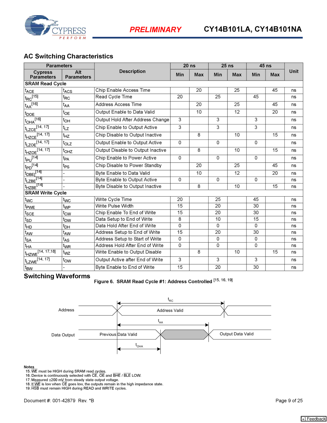
Figure 6. SRAM Read Cycle #1: Address Controlled [15, 16, 19]
| tRC |
Address | Address Valid |
| tAA |
Data Output | Previous Data Valid |
| tOHA |
Notes
15.WE must be HIGH during SRAM read cycles.
16.Device is continuously selected with CE, OE and BHE / BLE LOW.
17.Measured ±200 mV from steady state output voltage.
18.If WE is low when CE goes low, the outputs remain in the high impedance state.
19.HSB must remain HIGH during READ and WRITE cycles.
Output Data Valid
Document #: | Page 9 of 25 |
[+] Feedback