PRELIMINARY
|
|
|
|
|
| CY14B104LA, CY14B104NA | ||
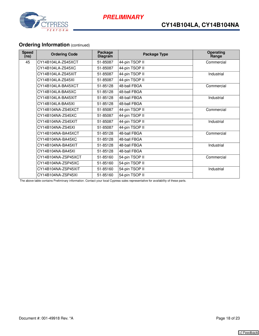
Ordering Information (continued) |
|
|
|
| ||||
|
|
|
|
|
|
|
| |
Speed | Ordering Code | Package | Package Type | Operating | ||||
(ns) | Diagram | Range | ||||||
|
|
|
|
| ||||
45 |
|
| Commercial | |||||
|
|
|
|
|
| |||
|
|
|
| |||||
|
|
|
|
|
| |||
|
|
| Industrial | |||||
|
|
|
|
|
| |||
|
|
|
| |||||
|
|
|
|
|
| |||
|
|
| Commercial | |||||
|
|
|
|
|
| |||
|
|
|
| |||||
|
|
|
|
|
| |||
|
|
| Industrial | |||||
|
|
|
|
|
| |||
|
|
|
| |||||
|
|
|
|
|
| |||
|
|
| Commercial | |||||
|
|
|
|
|
| |||
|
|
|
| |||||
|
|
|
|
|
| |||
|
|
| Industrial | |||||
|
|
|
|
|
| |||
|
|
|
| |||||
|
|
|
|
|
| |||
|
|
| Commercial | |||||
|
|
|
|
|
| |||
|
|
|
| |||||
|
|
|
|
|
| |||
|
|
| Industrial | |||||
|
|
|
|
|
| |||
|
|
|
| |||||
|
|
|
|
|
| |||
|
|
| Commercial | |||||
|
|
|
|
|
| |||
|
|
|
| |||||
|
|
|
|
|
| |||
|
|
| Industrial | |||||
|
|
|
|
|
| |||
|
|
|
| |||||
|
|
|
|
|
|
|
| |
The above table contains Preliminary information. Contact your local Cypress sales representative for availability of these parts.
Document #: | Page 18 of 23 |
[+] Feedback