Contents
CY14B104LA, CY14B104NA
Features
Logic Block Diagram1, 2
PRELIMINARY
not to scale
Pinouts
9 44 - TSOP
12 Top View 13 not to scale
Pin Definitions
CY14B104LA, CY14B104NA
PRELIMINARY
AutoStore Operation
Device Operation
SRAM Read
SRAM Write
PRELIMINARY
Hardware RECALL Power Up
Software STORE
Software RECALL
PRELIMINARY
Preventing AutoStore
Data Protection
Noise Considerations
+ Feedback
Best Practices
PRELIMINARY
CY14B104LA, CY14B104NA
PRELIMINARY
DC Electrical Characteristics
Maximum Ratings
Operating Range
AC Test Conditions
Data Retention and Endurance
Capacitance
Thermal Resistance
CY14B104LA, CY14B104NA
AC Switching Characteristics
Switching Waveforms
PRELIMINARY
Figure 8. SRAM Write Cycle #1 WE Controlled3, 16
PRELIMINARY
CY14B104LA, CY14B104NA
Figure 7. SRAM Read Cycle #2 CE and OE Controlled3, 13
Figure 10. SRAM Write Cycle #3 BHE and BLE Controlled 3, 16, 17
PRELIMINARY
CY14B104LA, CY14B104NA
Figure 9. SRAM Write Cycle #2 CE Controlled3, 16
CY14B104LA, CY14B104NA
AutoStore/Power Up RECALL
Switching Waveforms
PRELIMINARY
CY14B104LA, CY14B104NA
Software Controlled STORE/RECALL Cycle
Switching Waveforms
PRELIMINARY
CY14B104LA, CY14B104NA
Hardware STORE Cycle
Switching Waveforms
PRELIMINARY
PRELIMINARY
For x8 Configuration
For x16 Configuration
Truth Table For SRAM Operations
PRELIMINARY
Ordering Information
CY14B104LA, CY14B104NA
PRELIMINARY
Ordering Information continued
CY14B104LA, CY14B104NA
CY 14 B 104 L A -ZS P 20 X C T
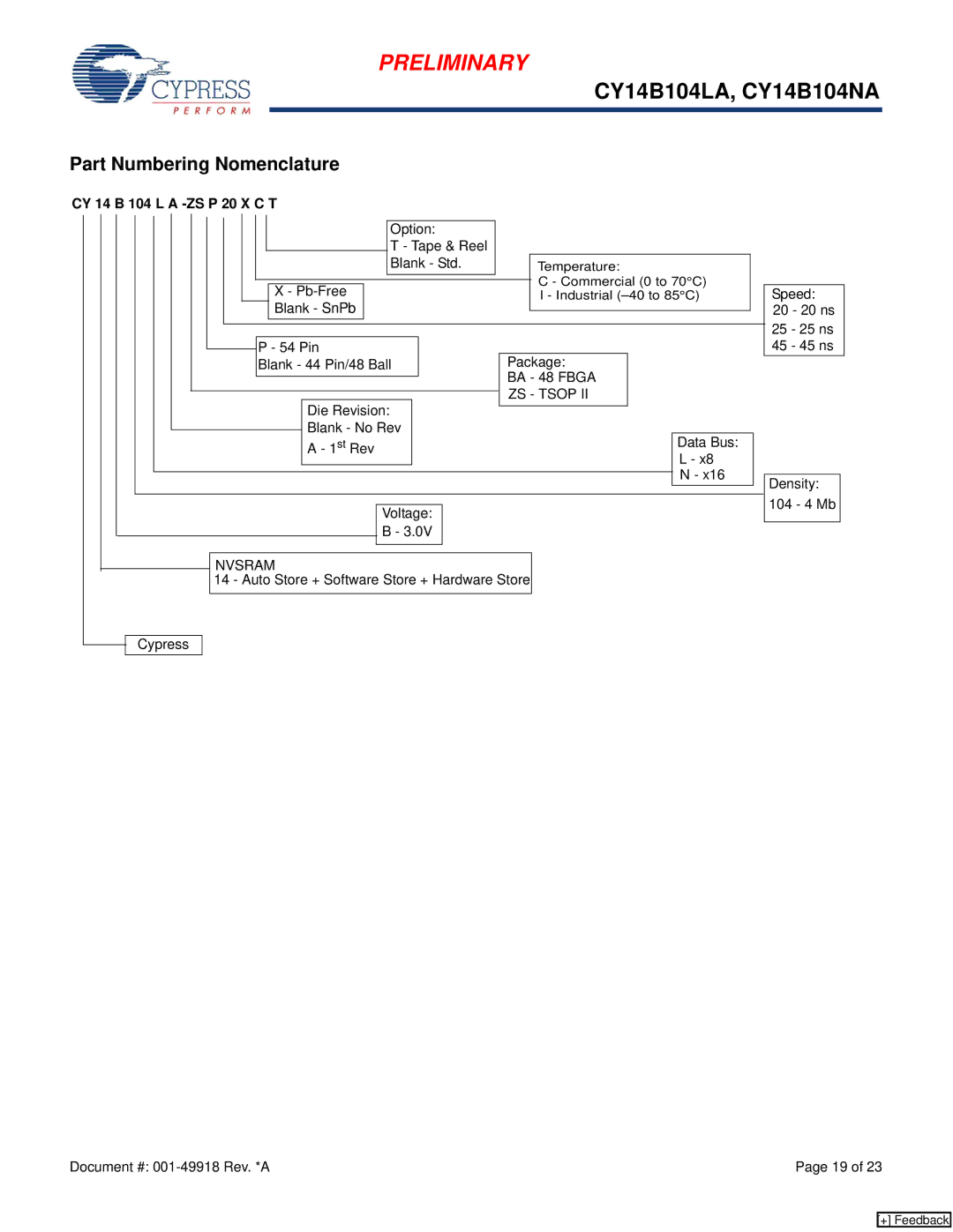
Part Numbering Nomenclature
PRELIMINARY
CY14B104LA, CY14B104NA
Figure 16. 44-Pin TSOP II
Package Diagrams
PRELIMINARY
CY14B104LA, CY14B104NA
Figure 17. 48-Ball FBGA - 6 mm x 10 mm x 1.2 mm
Package Diagrams continued
PRELIMINARY
CY14B104LA, CY14B104NA
Figure 18. 54-Pin TSOP
Package Diagrams continued
PRELIMINARY
CY14B104LA, CY14B104NA
Worldwide Sales and Design Support
Sales, Solutions, and Legal Information
PSoC Solutions
Document History Page