PRELIMINARY
CY14B104LA, CY14B104NA
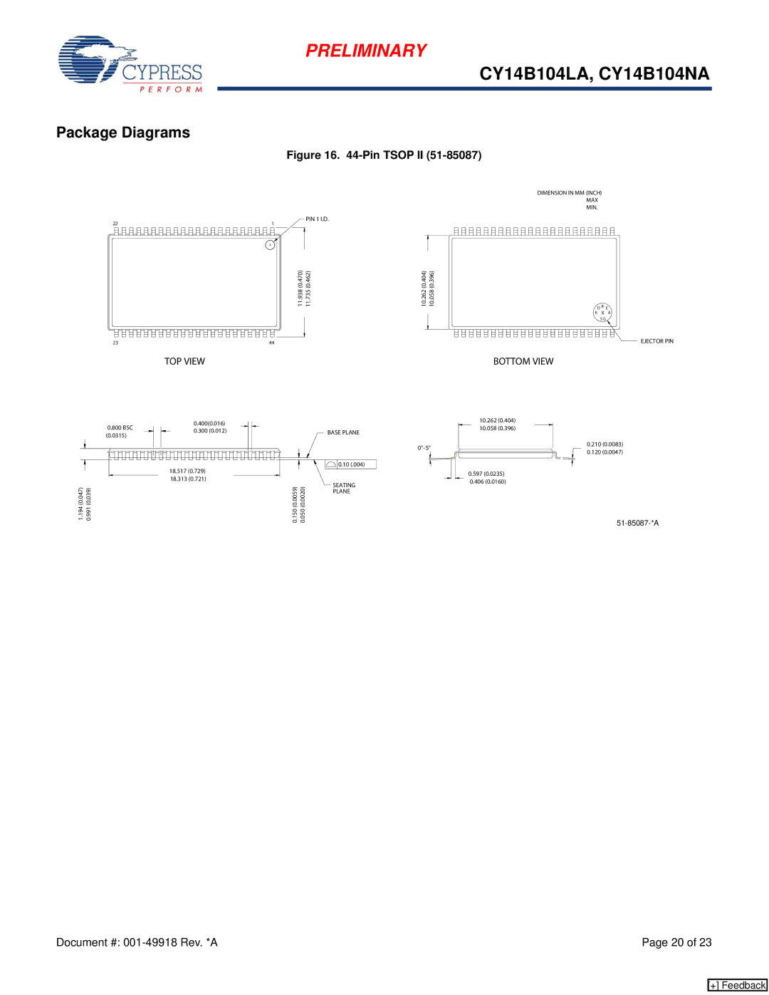
Package Diagrams
Figure 16. 44-Pin TSOP II (51-85087)
22 | 1 | PIN 1 I.D. |
|
|
|
|
| ||
| 11.938 (0.470) | 11.735 (0.462) | 10.262 (0.404) | 10.058 (0.396) |
23 | 44 |
|
|
|
DIMENSION IN MM (INCH)
MAX
MIN.
O R E
K X A
S G
EJECTOR PIN
TOP VIEW | BOTTOM VIEW |
0.800 BSC | 0.400(0.016) |
| |
0.300 (0.012) | BASE PLANE | ||
(0.0315) | |||
|
|
0°
0.10 (.004) |
18.517 (0.729) |
18.313 (0.721) |
(0.047)1.194 | (0.039)0.991 | (0.0059)0.150 | (0.0020)0.050 |
| SEATING |
| |||||
| PLANE | ||||
|
|
|
|
|
10.262 (0.404)
10.058 (0.396)
0.597 (0.0235)
0.406 (0.0160)
0.210 (0.0083)
0.120 (0.0047)
Document #: | Page 20 of 23 |
[+] Feedback