PRELIMINARY
CY14B104LA, CY14B104NA
Device Operation
The CY14B104LA/CY14B104NA nvSRAM is made up of two functional components paired in the same physical cell. They are a SRAM memory cell and a nonvolatile QuantumTrap cell. The SRAM memory cell operates as a standard fast static RAM. Data in the SRAM is transferred to the nonvolatile cell (the STORE operation), or from the nonvolatile cell to the SRAM (the RECALL operation). Using this unique architecture, all cells are stored and recalled in parallel. During the STORE and RECALL operations, SRAM read and write operations are inhibited. The CY14B104LA/CY14B104NA supports infinite reads and writes similar to a typical SRAM. In addition, it provides infinite RECALL operations from the nonvolatile cells and up to 200K STORE operations. See the Truth Table For SRAM Operations on page 16 for a complete description of read and write modes.
SRAM Read
The CY14B104LA/CY14B104NA performs a read cycle when CE and OE are LOW and WE and HSB are HIGH. The address specified on pins
SRAM Write
A write cycle is performed when CE and WE are LOW and HSB is HIGH. The address inputs must be stable before entering the write cycle and must remain stable until CE or WE goes HIGH at the end of the cycle. The data on the common I/O pins
AutoStore Operation
The CY14B104LA/CY14B104NA stores data to the nvSRAM using one of the following three storage operations: Hardware Store activated by HSB; Software Store activated by an address sequence; AutoStore on device power down. The AutoStore operation is a unique feature of QuantumTrap technology and is enabled by default on the CY14B104LA/CY14B104NA.
During a normal operation, the device draws current from VCC to charge a capacitor connected to the VCAP pin. This stored charge is used by the chip to perform a single STORE operation. If the voltage on the VCC pin drops below VSWITCH, the part automatically disconnects the VCAP pin from VCC. A STORE operation is initiated with power provided by the VCAP capacitor.
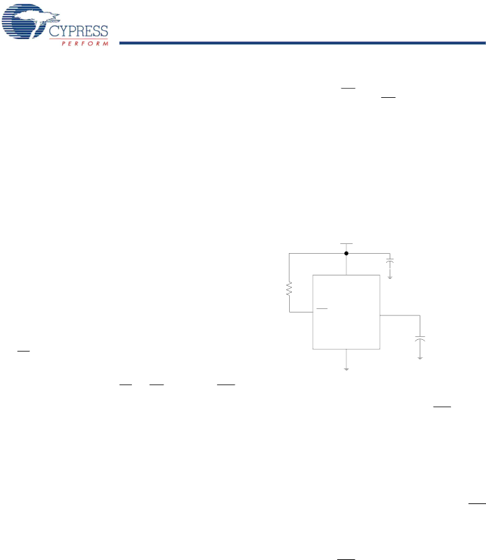
Figure 4 shows the proper connection of the storage capacitor (VCAP) for automatic store operation. Refer to DC Electrical
Characteristics on page 8 for the size of VCAP. The voltage on the VCAP pin is driven to VCC by a regulator on the chip. A pull up should be placed on WE to hold it inactive during power up. This pull up is effective only if the WE signal is tri-state during power up. Many MPUs tri-state their controls on power up. This should be verified when using the pull up. When the nvSRAM comes out of power-on-recall, the MPU must be active or the WE held inactive until the MPU comes out of reset.
To reduce unnecessary nonvolatile stores, AutoStore and hardware store operations are ignored unless at least one write operation has taken place since the most recent STORE or RECALL cycle. Software initiated STORE cycles are performed regardless of whether a write operation has taken place. The HSB signal is monitored by the system to detect if an AutoStore cycle is in progress.
Figure 4. AutoStore Mode
| Vcc | |
10kOhm | 0.1uF | |
Vcc | ||
| ||
WE | VCAP | |
| VCAP | |
| VSS |
Hardware STORE Operation
The CY14B104LA/CY14B104NA provides the HSB[6] pin to control and acknowledge the STORE operations. Use the HSB pin to request a hardware STORE cycle. When the HSB pin is driven LOW, the CY14B104LA/CY14B104NA conditionally initiates a STORE operation after tDELAY. An actual STORE cycle only begins if a write to the SRAM has taken place since the last STORE or RECALL cycle. The HSB pin also acts as an open drain driver that is internally driven LOW to indicate a busy condition when the STORE (initiated by any means) is in progress.
SRAM read and write operations that are in progress when HSB is driven LOW by any means are given time to complete before the STORE operation is initiated. After HSB goes LOW, the CY14B104LA/CY14B104NA continues SRAM operations for tDELAY. If a write is in progress when HSB is pulled LOW it is enabled a time, tDELAY to complete. However, any SRAM write cycles requested after HSB goes LOW are inhibited until HSB returns HIGH. In case the write latch is not set, HSB is not driven LOW by the CY14B104LA/CY14B104NA. But any SRAM read and write cycles are inhibited until HSB is returned HIGH by MPU or other external source.
During any STORE operation, regardless of how it is initiated, the CY14B104LA/CY14B104NA continues to drive the HSB pin LOW, releasing it only when the STORE is complete. When the STORE operation is completed, the CY14B104LA/CY14B104NA
Document #: | Page 4 of 23 |
[+] Feedback