PRELIMINARY
CY14B104LA, CY14B104NA
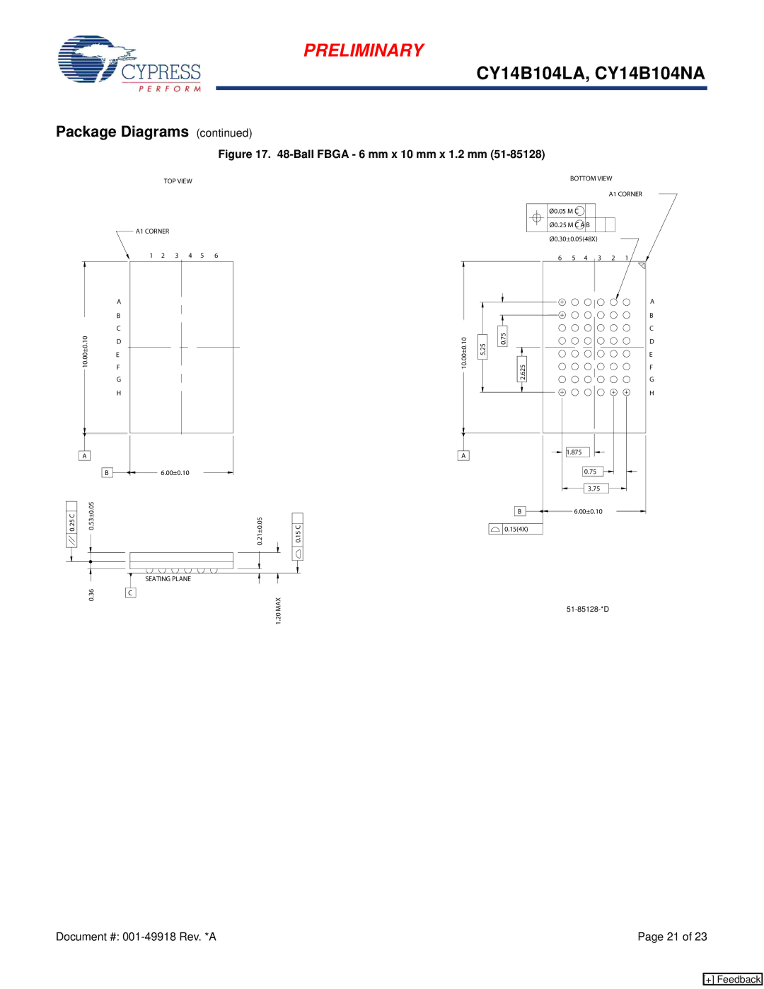
Package Diagrams (continued)
Figure 17. 48-Ball FBGA - 6 mm x 10 mm x 1.2 mm (51-85128)
TOP VIEW
A1 CORNER
1 2 3 4 5 6
BOTTOM VIEW
A1 CORNER
Ø0.05 M C |
|
|
|
| |
Ø0.25 M C A B |
|
|
| ||
Ø0.30±0.05(48X) |
|
|
| ||
6 | 5 | 4 | 3 | 2 | 1 |
|
| A | |
|
| B | |
|
| ||
10.00±0.10 | C | ||
D | |||
|
| ||
|
| E | |
|
| F | |
|
| G | |
|
| H | |
|
|
| |
|
|
|
|
|
|
|
|
|
| A |
|
|
| ||
|
|
|
|
|
|
|
|
|
|
|
|
|
| B |
|
|
| 0.53±0.05 |
|
| |||
|
|
| |||||
0.25 C | |||||||
|
|
|
|
|
|
|
|
|
|
|
|
|
|
|
|
|
|
|
|
|
|
|
|
|
|
|
|
|
|
|
|
|
|
|
|
|
|
|
|
|
|
|
|
|
|
|
|
0.36
6.00±0.10
0.21±0.05 |
|
|
|
|
|
| ||
|
|
| 0.15 C | |||||
|
|
|
|
|
|
|
|
|
|
|
|
|
|
|
|
|
|
SEATING PLANE
C
1.20 MAX
10.00±0.10
A
|
| A | |
|
| B | |
| 0.75 | C | |
5.25 | D | ||
E | |||
|
| ||
| 2.625 | F | |
| G | ||
|
| ||
|
| H | |
|
| 1.875 | |
|
| 0.75 | |
|
| 3.75 | |
| B | 6.00±0.10 | |
| 0.15(4X) |
| |
|
|
Document #: | Page 21 of 23 |
[+] Feedback