Manuals
/
Brands
/
Computer Equipment
/
Computer Hardware
/
Cypress
/
Computer Equipment
/
Computer Hardware
Cypress
CY7C1441AV33, CY7C1443AV33, CY7C1447AV33
- page 29
1
29
31
31
Download
31 pages, 906.77 Kb
CY7C1441AV33
CY7C1443AV33,CY7C1447AV33
Document #: 38-05357 Rev. *G
Page 29 of 31
Figure 3. 209-ball FBGA (14 x 22 x1.76 mm) (51-85167)
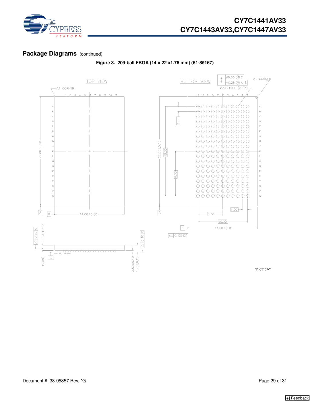
Package Diagrams
(continued)
51-85167-**
[+] Feedback
Contents
Main
36-Mbit (1M x 36/2M x 18/512K x 72) Flow-Through SRAM
CY7C1441AV33 CY7C1443AV33,CY7C1447AV33
Features
Functional Description
Selection Guide
Logic Block Diagram CY7C1441AV33 (1M x 36)
Logic Block Diagram CY7C1443AV33 (2Mx 18)
CE
ADDRESS REGISTER ADV CLK
BURST COUNTER AND LOGIC CLR
CY7C1441AV33 CY7C1443AV33,CY7C1447AV33
Document #: 38-05357 Rev. *G Page 3 of 31
Logic Block Diagram CY7C1447AV33 (512K x 72)
BYTE
MODE
CY7C1441AV33 CY7C1443AV33,CY7C1447AV33
Pin Configurations
Figure 1. 100-Pin TQFP Pinout
CY7C1441AV33 (1Mx 36)
CY7C1443AV33 (2M x 18)
Pin Configurations
165-ball FBGA (15 x 17 x 1.4 mm) Pinout CY7C1441AV33 (1M x 36)
CY7C1443AV33 (2M x 18)
2345671 A B C D E F G H J K L M N P R
891011
Pin Configurations
209-ball FBGA (14 x 22 x 1.76 mm) Pinout CY7C1447AV33 (512K 72)
CY7C1441AV33 CY7C1443AV33,CY7C1447AV33
Pin Definitions
Functional Overview
Single Read Accesses
Single Write Accesses Initiated by ADSP
Single Write Accesses Initiated by ADSC
Burst Sequences
ZZ Mode Electrical Characteristics
Truth Table
Partial Truth Table for Read/Write
Truth Table for Read/Write
IEEE 1149.1 Serial Boundary Scan (JTAG)
Disabling the JTAG Feature
Test Access Port (TAP)
Performing a TAP Reset
TAP Registers
TAP Instruction Set
CY7C1441AV33 CY7C1443AV33,CY7C1447AV33
TAP Ti min g
TAP AC Switching Characteristics
3.3V TAP AC Test Conditions
2.5V TAP AC Test Conditions
50
DO
T
Identification Register Definitions
Scan Register Sizes
Identification Codes
165-ball FBGA Boundary Scan Order
Maximum Ratings
Operating Range
Electrical Characteristics
DC Electrical Characteristics Over the Operating Range
Parameter Description Test Conditions Min. Max. Unit
Capacitance
Thermal Resistance
Switching Characteristics
Timing Diagrams
Figure 3. Read Cycle Timing
Figure 4. Write Cycle Timing[24, 25]
Figure 5. Read/Write Cycle Timing
Figure 6. ZZ Mode Timing
Ordering Information
Package Diagrams
Figure 1. 100-pin TQFP (14 x 20 x 1.4 mm) (51-85050)
A
Figure 2. 165-ball FBGA (15 x 17 x 1.4 mm) (51-85165)
Package Diagrams
51-85165-*A
Page
Document History Page