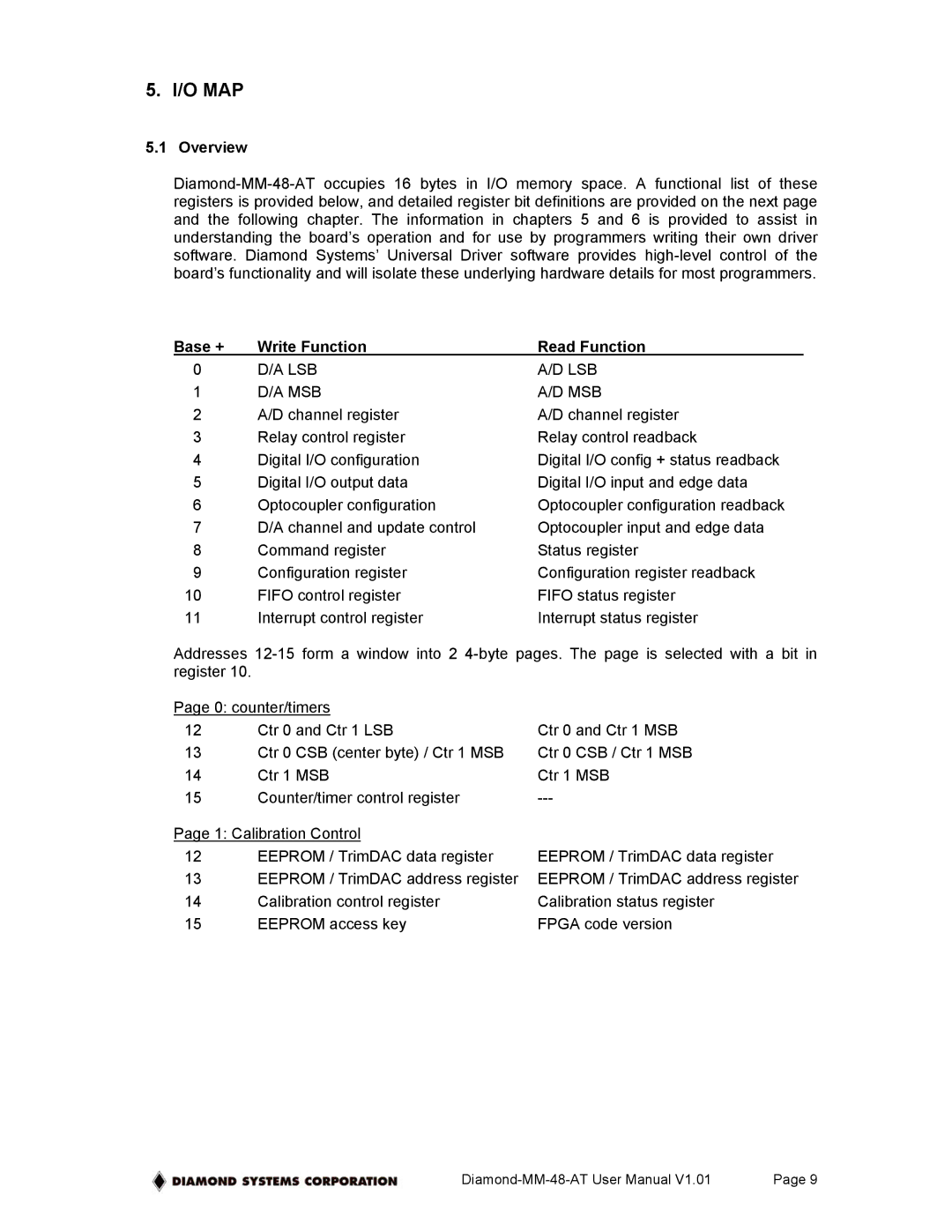
5. I/O MAP
5.1 Overview
Base + | Write Function | Read Function |
0 | D/A LSB | A/D LSB |
1 | D/A MSB | A/D MSB |
2 | A/D channel register | A/D channel register |
3 | Relay control register | Relay control readback |
4 | Digital I/O configuration | Digital I/O config + status readback |
5 | Digital I/O output data | Digital I/O input and edge data |
6 | Optocoupler configuration | Optocoupler configuration readback |
7 | D/A channel and update control | Optocoupler input and edge data |
8 | Command register | Status register |
9 | Configuration register | Configuration register readback |
10 | FIFO control register | FIFO status register |
11 | Interrupt control register | Interrupt status register |
Addresses
Page 0: counter/timers |
| |
12 | Ctr 0 and Ctr 1 LSB | Ctr 0 and Ctr 1 MSB |
13 | Ctr 0 CSB (center byte) / Ctr 1 MSB | Ctr 0 CSB / Ctr 1 MSB |
14 | Ctr 1 MSB | Ctr 1 MSB |
15 | Counter/timer control register | |
Page 1: Calibration Control |
| |
12 | EEPROM / TrimDAC data register | EEPROM / TrimDAC data register |
13 | EEPROM / TrimDAC address register | EEPROM / TrimDAC address register |
14 | Calibration control register | Calibration status register |
15 | EEPROM access key | FPGA code version |
Page 9 |
