
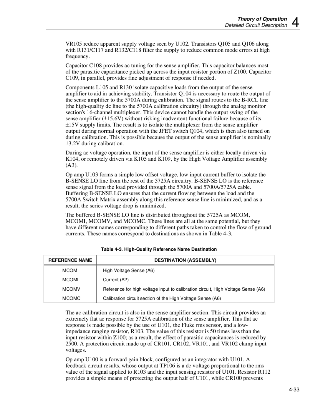
5725A specifications
The Fluke 5725A is a high-performance, multifunctional temperature calibration source designed to meet the demanding requirements of laboratory and industrial environments. Renowned for its accuracy, reliability, and versatility, the 5725A serves as a powerful tool for engineers and technicians engaged in temperature calibration processes.At the core of the 5725A is its advanced measurement technology, which allows for precision temperature calibrations across a wide range. With an operating temperature range from -200°C to 660°C, it caters to various applications, making it suitable for calibrating thermocouples, resistance temperature detectors (RTDs), and other temperature measurement devices.
One of the standout features of the Fluke 5725A is its outstanding accuracy, boasting a specified uncertainty of just ±0.15°C. This level of precision ensures that users can maintain compliance with regulatory standards and regulatory requirements in fields such as aerospace, pharmaceuticals, and manufacturing.
The Fluke 5725A is equipped with dual-channel capabilities, allowing users to calibrate two devices simultaneously. This enhances productivity by minimizing downtime and optimizing workflow efficiency. The intuitive touchscreen interface simplifies operations, enabling users to view measurements, set up test parameters, and access historical data with ease.
Versatile connectivity options such as USB and Ethernet enable seamless integration into existing systems and allow for data transfer, remote control, and configuration. This feature empowers technicians to conduct calibrations efficiently, whether on-site or remotely.
The robust design of the Fluke 5725A ensures its durability in demanding environments. Built with high-quality materials, it is resistant to shocks and vibrations, making it suitable for use in manufacturing plants and laboratories where equipment may be subjected to harsh conditions.
Another notable characteristic of the 5725A is its ability to generate stable temperature outputs with minimal drift, contributing to consistency in calibration results. Its built-in self-test functionality helps ensure that the unit remains in peak operating condition, giving users confidence in their calibration processes.
In summary, the Fluke 5725A is a top-tier temperature calibration source that excels in accuracy, reliability, and user-friendliness. Whether in laboratory settings or industrial applications, its advanced technologies and features make it an essential tool for professionals tasked with maintaining precision in temperature measurements.