Chapter 3 Jumpers and Switches
3.11 External Flash memory (JP: 49, 52, 56)
The
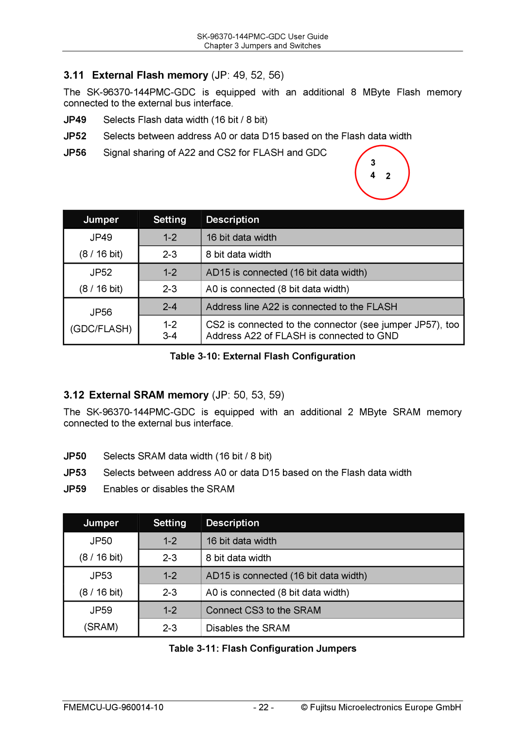
JP49 Selects Flash data width (16 bit / 8 bit)
JP52 Selects between address A0 or data D15 based on the Flash data width JP56 Signal sharing of A22 and CS2 for FLASH and GDC
3 |
|
4 | 2 |
| Jumper | Setting |
|
| Description |
| JP49 |
|
| 16 bit data width | |
| (8 / 16 bit) |
|
| 8 bit data width | |
|
|
|
|
|
|
| JP52 |
|
| AD15 is connected (16 bit data width) | |
| (8 / 16 bit) |
|
| A0 is connected (8 bit data width) | |
|
|
|
|
|
|
| JP56 |
|
| Address line A22 is connected to the FLASH | |
|
|
| CS2 is connected to the connector (see jumper JP57), too | ||
| (GDC/FLASH) |
|
| ||
|
|
| Address A22 of FLASH is connected to GND | ||
|
|
|
| ||
|
|
|
|
|
|
Table 3-10: External Flash Configuration
3.12 External SRAM memory (JP: 50, 53, 59)
The
JP50 Selects SRAM data width (16 bit / 8 bit)
JP53 Selects between address A0 or data D15 based on the Flash data width JP59 Enables or disables the SRAM
Jumper | Setting | Description |
JP50 | 16 bit data width | |
(8 / 16 bit) | 8 bit data width | |
|
|
|
JP53 | AD15 is connected (16 bit data width) | |
(8 / 16 bit) | A0 is connected (8 bit data width) | |
|
|
|
JP59 | Connect CS3 to the SRAM | |
(SRAM) | Disables the SRAM | |
|
|
|
Table 3-11: Flash Configuration Jumpers
- 22 - | © Fujitsu Microelectronics Europe GmbH |
