Hardware and Bios Technical Reference Manual
Hewlett-Packard Company
Preface
Ordering the Phoenix Bios Manual
Bibliography
Conventions
Contents
Overview
Bios version GX.07.xx
System Board Ns D3657-63001 and D3661-63001
Cache Memory Main Memory
Summary of the HP/Phoenix Bios
Video Controllers
Index
HP Vectra 500 Series
Introduction
Introduction
D4051-63001 Minitower Models
System Overview
D4051-63001 Models
D4051-63001- Desktop Models
D3657-63001 Minitower Models
D3657-63001 Models
D3657-63001 Desktop Models
Shading Description
System Features
D3661-63001 Model
D3661-63001 Minitower Model
HP Service Part Number
Component Desktop Minitower
Principal Features
Computer Characteristic Type Description
Physical and Environmental Specifications
Inches by 7 inches by 1.3 inches
These Operating temperature +5C to +40C +40F to +104F
Kcal per hour 360 BTU per hour
Keyboard Flat
+ 5 5A maximum per slot + 12 1A maximum per slot
Power Consumption
+ 5
+ 12
Parallel Device Connector
Rear Panel Connectors
Display Connector
CD-ROM Drive Specifications
HP Vectra 500 Series
System Board SiS Chipset Part Number D4051-63001
Overview
Overview
Supported Processor P54CS Level-2 L2 256 KB cache sockets
Configuration
System Board Architecture
System Board Architecture
System Board Physical Layout
Bios
SiS Chipset
SiS Chipset
SiS
Pentium Processor
Level-2 Cache Host Bridge & Memory Controller SiS
Control Main Memory Video
EDO Dram
Host/PCI Bridge SiS 5511 Chip
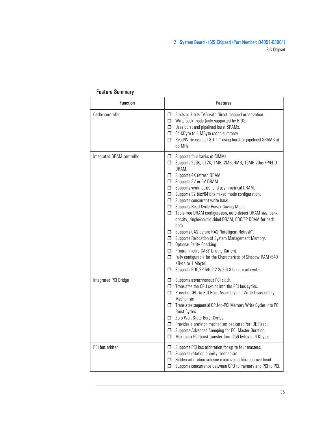
Feature Summary
PCI/ISA Bridge SiS 5513 Chip
Data Path SiS 5512 Chip
Interrupt Controller
Timer/Counter
ISA Bus Controller
DMA Controller
Switch Default
System Board Switches and Jumpers D4051-63001
SW1 Switch
Processor Speeds
SW2 Switch
Jumper J7 Settings
CPU Bus Frequency Jumper
Synchronous Asynchronous
Space-Bar Power-On Feature Jumper
Power-on Spacebar enabled Spacebar disabled
Cache Jumper
Memory Sockets D4051-63001
Processor Socket D4051-63001
Desktop Backplane
Backplane D4051-63001
ISA PCI
Minitower Backplane
Memory Total 12 MB
Devices on the Processor Local Bus D4051-63001
Main Memory UMA
Cache Memory D4051-63001
Pentium Processor D4051-63001
Level-1 Cache Memory
Level-2 Cache Memory
Instruction and Data Cache
Superscalar Architecture
Floating Point Unit
Dynamic Branch Prediction
Data Integrity
Advanced Power Management
Devices on the PCI Bus
Devices on the PCI Bus
Graphics/Integrated Video D4051-63001
Video Controller
Desktop Minitower
Desktop Configuration Connections to Data Cables
Integrated Drive Electronics IDE Controller
Mode
Configuration Connections to Data Cables
Transfer Rates Versus Modes of Operation
Bytes per
Disk Capacity Versus Modes of Addressing
Cylinders Heads per
Functions
Devices on the ISA Bus
Super I/O Chip NS 87308 or NS
Function Features
Serial/Parallel Ports
Keyboard and Mouse Controller
Floppy Drive Controller
Flash ROM
Bios version GX.07.xx
HP Setup Program
Bios version GX.07.xx
System Board Ns D3657-63001 and D3661-63001
Minitower Models
Desktop Models
D3661-63001 Models
Configuration Summary
IDE Controller Channel
Pentium Processor 256 KB Level-Two Cache Local Bus
PCI Bus
IDE Controller Channel Video
System Board Physical Layout
Host Bus
Principal Components and Features
Principal Components and Features
PCI Chipset
PCI, Cache and Memory Controller SB82437FX-66
SB82437FX-66 Feature Summary
Optional buffering of PCI memory writes
Data Path Unit SB82438FX
Memory address map
Pentium reads and writes
PCI/ISA Bridge and IDE Controller SB82371FB
SB82438FX and SB82371FB Feature Summary
System Board Configuration Switches
Main Memory Sockets
Processor Socket
VRM Socket
HP Vectra 500 Series Desktop Backplane
Advanced Power Management APM
HP Vectra 500 Series Minitower Backplane
Devices on the Processor Local Bus
Devices on the Processor Local Bus
Pentium Processor
Floating Point Unit FPU
Bus Frequencies
Switch
Closed 200 MHz
Cache Memory
166 MHz
180 MHz
Main Memory
Video Controller
Video Dram
Video Resolutions Supported
S3 Trio 64PnP Video Controller
Other PCI Accessory Devices
Serial/Parallel Communications Ports
Super I/O Chip SMC FDC37C932
Serial Eeprom
Floppy Drive Controller FDC
Real-Time Clock RTC
System ROM
Other ISA Accessory Devices
Summary of the HP/Phoenix Bios
Updating the System ROM
HP/Phoenix Bios Description
HP/Phoenix Bios Description
Error Diagnostics and Suggested Corrective Actions
Little Ben
HP/Phoenix Bios Bios version GX.07.xx
HP/Phoenix Bios Bios version GX.07.xx
Setup Program Bios version GX.07.xx
Main Menu Bios version GX.07.xx
Parallel port 378h IRQ7 On board parallel port
Configuration Menu Bios version GX.07.xx
Configuration T e g r a t e d I / O P o r t s
Enables or disables
Security Menu Bios version GX.07.xx
Summary Configuration Screen Bios version GX.07.xx
Power Menu Bios version GX.07.xx
Bank B 8MB EDO
PCI Slot Not Installed ISA PnP
System RAM 15 MB
Bank a MB EDO
System Memory Map Bios version GX.07.xx
Addresses Used by the System Bios version GX.07.xx
Address Ports Function Bits
Bios I/O Port Map Bios version GX.07.xx
0378-037F Parallel port 03B0-03BB
System Board Components Bios version GX.07.xx
DMA Channel Controllers Bios version GX.07.xx
Used for PCI configuration1
IRQ Interrupt Vector Interrupt Request Description
Interrupt Controllers
First DMA controller used for 8-bit transfers
Second DMA controller used for 16-bit transfers
Power-On Self-Test Bios version GX.07.xx
PCI Interrupt Request Lines Bios version GX.07.xx
Process to abort
Test Description System Bios Tests
Abort
To abort
Internal Cache
Display, but the boot process continues
Using
Failure causes an error code to display
Error Messages Bios version GX.07.xx
Message Corrective Action and/or Explanation
Numeric Beep Pattern Code Description
Beep Codes Bios version GX.07.xx
HP/Phoenix Bios Bios version GJ.07.xx
HP/Phoenix Bios Bios version GJ.07.xx
Setup Program Bios version GJ.07.xx
Main Menu Bios version GJ.07.xx
Configuration Menu Bios version GJ.07.xx
Preferences Menu Bios version GJ.07.xx
102
Security Menu Bios version GJ.07.xx
Power Menu Bios version GJ.07.xx
Copyright 1995 Hewlett-Packard
Summary Configuration Screen Bios version GJ.07.xx
104
Addresses Used by the System Bios version GJ.07.xx
System Memory Map Bios version GJ.07.xx
MB plus- Extended Memory
105
Bios I/O Port Map Bios version GJ.07.xx
0378-037F Parallel Port 03B0-03DF
106
DMA Channel Controllers Bios version GJ.07.xx
Used for PCI Configuration1 0496-0497 HP Reserved 0678-067A
0778-077A
107
108
PCI Interrupt Request Lines
Free, if not used used for serial port2
Free, if not used used for parallel port3
109
Power-On Self-Test Bios version GJ.07.xx
Shadow Ram Bios version GJ.07.xx
Initialize the Video
Error code to display and the boot process to abort
Post Test
Video Tests
Code to display 111
System Board Tests
Test failure causes an error code to display
Causes an error code to display
Processor. Test failure causes an error code to display
Ports. Test failure causes an error code to display
113
Error Messages Bios version GJ.07.xx
Device 0079 on system board
114
Beep Codes Bios version GJ.07.xx
Message
115
Video Controllers
116
SiS 6205 Video Controller
SiS 6205 Video Controller Summary
SiS 6205 Video Controller
Upgrading Video Memory UMA
Upgradeable to
Memory
Using the HP Dynamic Video Feature
Typical Windows 95 Video Resolutions SiS 6205 Chip
Resolution Number of colors
119
Vesa Feature Connector SiS 6205 Chip
S3 Trio 64 Video Controller Summary
Upgradeable
Integrated Ultra VGA Video Controller
121
S3 Trio 64 Video Memory
S3 Trio 64 Video Modes
122
Extended Video Modes with 1 MB Dram S3 Trio
123
Mode No
124
640 x 256, 64K 60, 72 800 x 56, 60, 72 1024 x I43 1 60, 70
Typical Windows 95 Video Resolutions S3 Trio
126
Vesa Connector
127
Matrox MGA Millennium Video Controller Card
Matrox MGA Millennium Video Controller Card
128
MGA Connectors
MGA Video Memory
640 x 256, 64K, 16M 120 800 x 1024 x 1280 x 1600 x 1200
Available MGA Video Resolutions
Resolution
Refresh Rate Hz
Number 256 64 K 16.7 M
256 64 K 16.7 M
131
MGA Video Bios
Further Information About MGA
132
DB15 Connector Pinout
DB15 Connector Pinout
Aztech AT3300 Audio Fax/Data Modem
134
135
Communications Options
136
Tone or pulse dialing
Configuring the firmware code
European Firmware and Telephone Line Configuration
138
Using the Aztech AT3300 Localisation Utility
Aztech AT3300 Localisation Utility
139
Select the Country
140
Using the HyperTerminal Application
Comments Modem
142
143
Index
S3 Trio
144
UMA
145
146