PC Processors (Mobile Celeron) - Fall 2001
Created by IBM PC Institute Personal Systems Reference (PSREF)
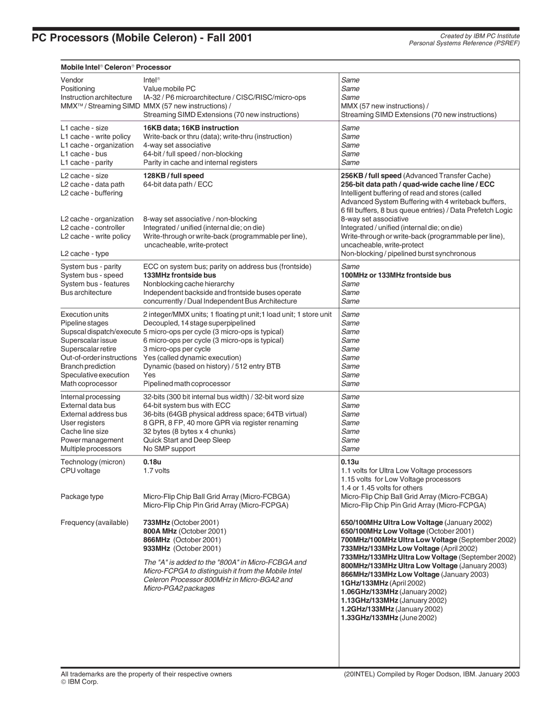
Mobile Intel→ Celeron→ Processor
Vendor | Intel→ | Same |
Positioning | Value mobile PC | Same |
Instruction architecture | Same | |
MMX™ / Streaming SIMD MMX (57 new instructions) / | MMX (57 new instructions) / | |
| Streaming SIMD Extensions (70 new instructions) | Streaming SIMD Extensions (70 new instructions) |
|
|
|
L1 cache - size | 16KB data; 16KB instruction | Same |
L1 cache - write policy | Same | |
L1 cache - organization | Same | |
L1 cache - bus | Same | |
L1 cache - parity | Parity in cache and internal registers | Same |
|
|
|
L2 cache - size | 128KB / full speed | 256KB / full speed (Advanced Transfer Cache) |
L2 cache - data path |
| |
L2 cache - buffering |
| Intelligent buffering of read and stores (called |
|
| Advanced System Buffering with 4 writeback buffers, |
|
| 6 fill buffers, 8 bus queue entries) / Data Prefetch Logic |
L2 cache - organization | ||
L2 cache - controller | Integrated / unified (internal die; on die) | Integrated / unified (internal die; on die) |
L2 cache - write policy | ||
| uncacheable, | uncacheable, |
L2 cache - type |
| |
|
|
|
System bus - parity | ECC on system bus; parity on address bus (frontside) | Same |
System bus - speed | 133MHz frontside bus | 100MHz or 133MHz frontside bus |
System bus - features | Nonblocking cache hierarchy | Same |
Bus architecture | Independent backside and frontside buses operate | Same |
| concurrently / Dual Independent Bus Architecture | Same |
|
|
|
Execution units | 2 integer/MMX units; 1 floating pt unit;1 load unit; 1 store unit | Same |
Pipeline stages | Decoupled, 14 stage superpipelined | Same |
Supscal dispatch/execute 5 | Same | |
Superscalar issue | 6 | Same |
Superscalar retire | 3 | Same |
Yes (called dynamic execution) | Same | |
Branch prediction | Dynamic (based on history) / 512 entry BTB | Same |
Speculative execution | Yes | Same |
Math coprocessor | Pipelined math coprocessor | Same |
|
|
|
Internal processing | Same | |
External data bus | Same | |
External address bus | Same | |
User registers | 8 GPR, 8 FP, 40 more GPR via register renaming | Same |
Cache line size | 32 bytes (8 bytes x 4 chunks) | Same |
Power management | Quick Start and Deep Sleep | Same |
Multiple processors | No SMP support | Same |
|
|
|
Technology (micron) | 0.18u | 0.13u |
CPU voltage | 1.7 volts | 1.1 volts for Ultra Low Voltage processors |
|
| 1.15 volts for Low Voltage processors |
|
| 1.4 or 1.45 volts for others |
Package type | ||
| ||
Frequency (available) | 733MHz (October 2001) | 650/100MHz Ultra Low Voltage (January 2002) |
| 800A MHz (October 2001) | 650/100MHz Low Voltage (October 2001) |
| 866MHz (October 2001) | 700MHz/100MHz Ultra Low Voltage (September 2002) |
| 933MHz (October 2001) | 733MHz/133MHz Low Voltage (April 2002) |
| The "A" is added to the "800A" in | 733MHz/133MHz Ultra Low Voltage (September 2002) |
| 800MHz/133MHz Ultra Low Voltage (January 2003) | |
| ||
| 866MHz/133MHz Low Voltage (January 2003) | |
| Celeron Processor 800MHz in | |
| 1GHz/133MHz (April 2002) | |
| ||
| 1.06GHz/133MHz (January 2002) | |
|
| |
|
| 1.13GHz/133MHz (January 2002) |
|
| 1.2GHz/133MHz (January 2002) |
|
| 1.33GHz/133MHz (June 2002) |
|
|
|
All trademarks are the property of their respective owners | (20INTEL) Compiled by Roger Dodson, IBM. January 2003 |
♥ IBM Corp. |
|