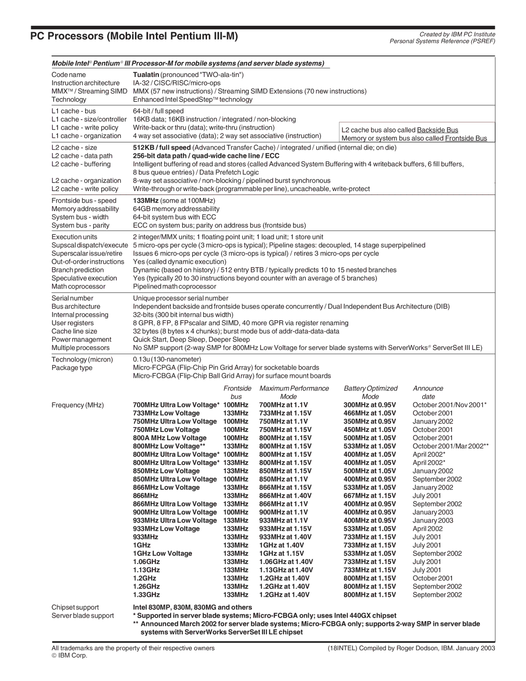
PC Processors (Mobile Intel Pentium | Created by IBM PC Institute | |
Personal Systems Reference (PSREF) | ||
|
Mobile Intel→ Pentium→ III
Code name | Tualatin (pronounced |
| |
Instruction architecture |
| ||
MMX™ / Streaming SIMD | MMX (57 new instructions) / Streaming SIMD Extensions (70 new instructions) | ||
Technology | Enhanced Intel SpeedStep™ technology |
| |
|
|
|
|
L1 cache - bus |
| ||
L1 cache - size/controller | 16KB data; 16KB instruction / integrated / |
| |
L1 cache - write policy |
| L2 cache bus also called Backside Bus | |
L1 cache - organization | 4 way set associative (data); 2 way set associative (instruction) |
| |
| Memory or system bus also called Frontside Bus | ||
|
|
| |
L2 cache - size | 512KB / full speed (Advanced Transfer Cache) / integrated / unified (internal die; on die) | ||
L2 cache - data path |
|
| |
L2 cache - buffering | Intelligent buffering of read and stores (called Advanced System Buffering with 4 writeback buffers, 6 fill buffers, | ||
| 8 bus queue entries) / Data Prefetch Logic |
| |
L2 cache - organization |
| ||
L2 cache - write policy | |||
|
|
|
|
Frontside bus - speed | 133MHz (some at 100MHz) |
| |
Memory addressability | 64GB memory addressability |
| |
System bus - width |
| ||
System bus - parity | ECC on system bus; parity on address bus (frontside bus) |
| |
|
|
|
|
Execution units | 2 integer/MMX units; 1 floating point unit; 1 load unit; 1 store unit |
| |
Supscal dispatch/execute | 5 | ||
Superscalar issue/retire | Issues 6 | ||
Yes (called dynamic execution) |
| ||
Branch prediction | Dynamic (based on history) / 512 entry BTB / typically predicts 10 to 15 nested branches | ||
Speculative execution | Yes (typically 20 to 30 instructions beyond counter with an average of 5 branches) | ||
Math coprocessor | Pipelined math coprocessor |
| |
|
|
|
|
Serial number | Unique processor serial number |
| |
Bus architecture | Independent backside and frontside buses operate concurrently / Dual Independent Bus Architecture (DIB) | ||
Internal processing |
| ||
User registers | 8 GPR, 8 FP, 8 FPscalar and SIMD, 40 more GPR via register renaming | ||
Cache line size | 32 bytes (8 bytes x 4 chunks); burst mode bus of |
| |
Power management | Quick Start, Deep Sleep, Deeper Sleep |
| |
Multiple processors | No SMP support | ||
Technology (micron) | 0.13u |
| |
Package type |
| ||
|
| ||
|
| Frontside | Maximum Performance |
|
| bus | Mode |
Frequency (MHz) | 700MHz Ultra Low Voltage* 100MHz | 700MHz at 1.1V | |
| 733MHz Low Voltage | 133MHz | 733MHz at 1.15V |
| 750MHz Ultra Low Voltage | 100MHz | 750MHz at 1.1V |
| 750MHz Low Voltage | 100MHz | 750MHz at 1.15V |
| 800A MHz Low Voltage | 100MHz | 800MHz at 1.15V |
| 800MHz Low Voltage** | 133MHz | 800MHz at 1.15V |
| 800MHz Ultra Low Voltage* | 100MHz | 800MHz at 1.15V |
| 800MHz Ultra Low Voltage* | 133MHz | 800MHz at 1.15V |
| 850MHz Low Voltage | 133MHz | 850MHz at 1.15V |
| 850MHz Ultra Low Voltage | 100MHz | 850MHz at 1.1V |
| 866MHz Low Voltage | 133MHz | 866MHz at 1.15V |
| 866MHz | 133MHz | 866MHz at 1.40V |
| 866MHz Ultra Low Voltage | 133MHz | 866MHz at 1.1V |
| 900MHz Ultra Low Voltage | 100MHz | 900MHz at 1.1V |
| 933MHz Ultra Low Voltage | 133MHz | 933MHz at 1.1V |
| 933MHz Low Voltage | 133MHz | 933MHz at 1.15V |
| 933MHz | 133MHz | 933MHz at 1.40V |
| 1GHz | 133MHz | 1GHz at 1.40V |
| 1GHz Low Voltage | 133MHz | 1GHz at 1.15V |
| 1.06GHz | 133MHz | 1.06GHz at 1.40V |
| 1.13GHz | 133MHz | 1.13GHz at 1.40V |
| 1.2GHz | 133MHz | 1.2GHz at 1.40V |
| 1.26GHz | 133MHz | 1.2GHz at 1.40V |
| 1.33GHz | 133MHz | 1.2GHz at 1.40V |
Battery Optimized | Announce |
Mode | date |
300MHz at 0.95V | October 2001/Nov 2001* |
466MHz at 1.05V | October 2001 |
350MHz at 0.95V | January 2002 |
450MHz at 1.05V | October 2001 |
500MHz at 1.05V | October 2001 |
533MHz at 1.05V | October 2001/Mar 2002** |
400MHz at 1.05V | April 2002* |
400MHz at 1.05V | April 2002* |
500MHz at 1.05V | January 2002 |
400MHz at 0.95V | September 2002 |
533MHz at 1.05V | January 2002 |
667MHz at 1.15V | July 2001 |
400MHz at 0.95V | September 2002 |
400MHz at 0.95V | January 2003 |
400MHz at 0.95V | January 2003 |
533MHz at 1.05V | April 2002 |
733MHz at 1.15V | July 2001 |
733MHz at 1.15V | July 2001 |
533MHz at 1.05V | September 2002 |
733MHz at 1.15V | July 2001 |
733MHz at 1.15V | July 2001 |
800MHz at 1.15V | October 2001 |
800MHz at 1.15V | September 2002 |
800MHz at 1.15V | September 2002 |
Chipset support | Intel 830MP, 830M, 830MG and others |
Server blade support | * Supported in server blade systems; |
| ** Announced March 2002 for server blade systems; |
| systems with ServerWorks ServerSet III LE chipset |
All trademarks are the property of their respective owners | (18INTEL) Compiled by Roger Dodson, IBM. January 2003 |
♥ IBM Corp. |
|