PC Processors (Pentium III - Tualatin) |
|
| Created by IBM PC Institute | |||
|
| Personal Systems Reference (PSREF) | ||||
|
|
|
|
|
| |
|
|
|
| |||
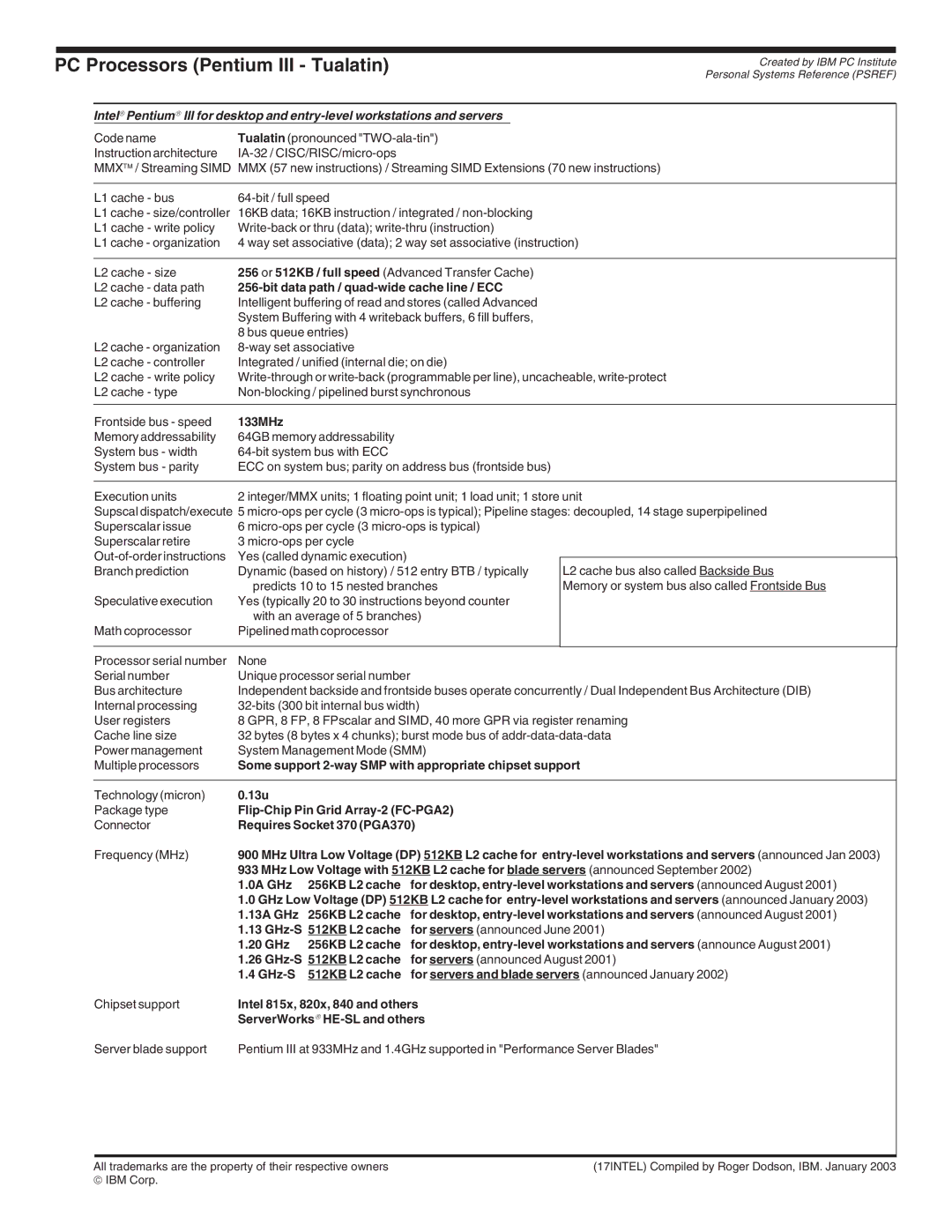
| Intel→ Pentium→ III for desktop and |
|
| |||
| Code name | Tualatin (pronounced |
| |||
| Instruction architecture |
|
|
| ||
| MMX™ / Streaming SIMD | MMX (57 new instructions) / Streaming SIMD Extensions (70 new instructions) | ||||
|
|
|
|
|
| |
| L1 cache - bus |
|
|
| ||
| L1 cache - size/controller | 16KB data; 16KB instruction / integrated / |
| |||
| L1 cache - write policy |
| ||||
| L1 cache - organization | 4 way set associative (data); 2 way set associative (instruction) | ||||
|
|
|
|
| ||
| L2 cache - size | 256 or 512KB / full speed (Advanced Transfer Cache) |
| |||
| L2 cache - data path |
|
| |||
| L2 cache - buffering | Intelligent buffering of read and stores (called Advanced |
| |||
|
| System Buffering with 4 writeback buffers, 6 fill buffers, |
| |||
|
| 8 bus queue entries) |
|
|
| |
| L2 cache - organization |
|
|
| ||
| L2 cache - controller | Integrated / unified (internal die; on die) |
| |||
| L2 cache - write policy | |||||
| L2 cache - type |
| ||||
|
|
|
|
|
|
|
| Frontside bus - speed | 133MHz |
|
|
|
|
| Memory addressability | 64GB memory addressability |
|
|
| |
| System bus - width |
|
|
| ||
| System bus - parity | ECC on system bus; parity on address bus (frontside bus) |
| |||
|
|
| ||||
| Execution units | 2 integer/MMX units; 1 floating point unit; 1 load unit; 1 store unit | ||||
| Supscal dispatch/execute 5 | |||||
| Superscalar issue | 6 |
| |||
| Superscalar retire | 3 |
|
|
| |
| Yes (called dynamic execution) |
|
|
| ||
|
|
| L2 cache bus also called Backside Bus | |||
| Branch prediction | Dynamic (based on history) / 512 entry BTB / typically | ||||
|
| predicts 10 to 15 nested branches | Memory or system bus also called Frontside Bus | |||
| Speculative execution | Yes (typically 20 to 30 instructions beyond counter |
| |||
|
| with an average of 5 branches) |
| |||
| Math coprocessor | Pipelined math coprocessor |
|
|
| |
|
|
|
|
|
|
|
| Processor serial number | None |
|
|
|
|
| Serial number | Unique processor serial number |
|
|
| |
| Bus architecture | Independent backside and frontside buses operate concurrently / Dual Independent Bus Architecture (DIB) | ||||
| Internal processing |
| ||||
| User registers | 8 GPR, 8 FP, 8 FPscalar and SIMD, 40 more GPR via register renaming | ||||
| Cache line size | 32 bytes (8 bytes x 4 chunks); burst mode bus of | ||||
| Power management | System Management Mode (SMM) |
| |||
| Multiple processors | Some support | ||||
|
|
|
|
|
|
|
| Technology (micron) | 0.13u |
|
|
|
|
| Package type |
|
| |||
| Connector | Requires Socket 370 (PGA370) |
| |||
| Frequency (MHz) | 900 MHz Ultra Low Voltage (DP) 512KB L2 cache for | ||||
|
| 933 MHz Low Voltage with 512KB L2 cache for blade servers (announced September 2002) | ||||
|
| 1.0A GHz | 256KB L2 cache | for desktop, | ||
|
| 1.0 GHz Low Voltage (DP) 512KB L2 cache for | ||||
|
| 1.13A GHz | 256KB L2 cache | for desktop, | ||
|
| 1.13 | for servers (announced June 2001) | |||
|
| 1.20 GHz | 256KB L2 cache | for desktop, | ||
|
| 1.26 | for servers (announced August 2001) | |||
|
| 1.4 | 512KB L2 cache | for servers and blade servers (announced January 2002) | ||
| Chipset support | Intel 815x, 820x, 840 and others |
| |||
|
| ServerWorks→ |
| |||
| Server blade support | Pentium III at 933MHz and 1.4GHz supported in "Performance Server Blades" | ||||
|
|
|
|
|
|
|
All trademarks are the property of their respective owners | (17INTEL) Compiled by Roger Dodson, IBM. January 2003 |
♥ IBM Corp. |
|