EM78M611E
Universal Serial Bus Series Microcontroller
After the PDA function is enabled (by setting IOCA[2] to 1), user can write a default value to the High Pattern counter register and Low Pattern counter register. Then set the corresponding interrupt enable bit (IOCF[5]). When the counting value of one “H” pattern is bigger than the default value of R11, the Pattern Detecting interrupt will be generated. Similarly, if the counting value of one “L” pattern is bigger than the default value of R10, Low Pattern Detecting interrupt will occur. Thus, the EM78M611 is notified and aware that one effective pattern is received from P.92.
If user does not need these two interrupts, they can be masked. The new value of counting a pattern will still be loaded to the R10 and R11. The firmware must poll and determine whether the value of these two registers has changed or not.
8.10 Pulse Width Modulation (PWM)
8.10.1 Function Description
In PWM mode, both PWM1 (P.92) and PWM2 (P.93) produce plus programmable signal of up to 8 bits resolution.
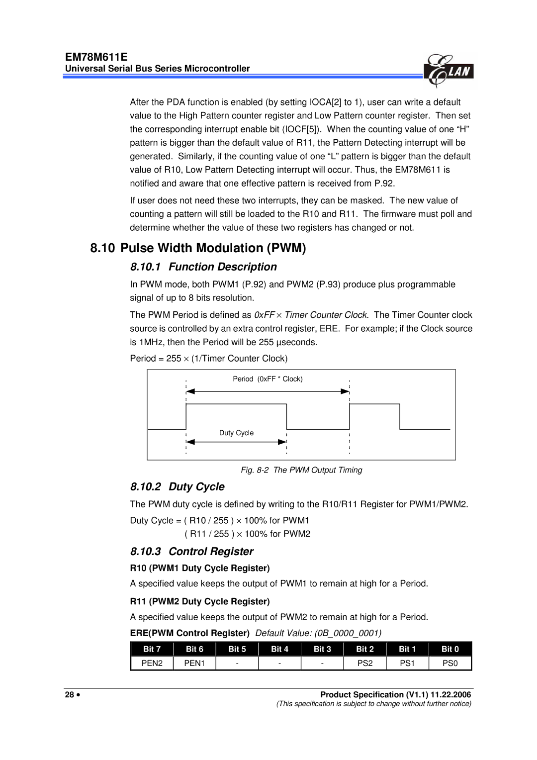
The PWM Period is defined as 0xFF ⋅ Timer Counter Clock. The Timer Counter clock source is controlled by an extra control register, ERE. For example; if the Clock source is 1MHz, then the Period will be 255 µseconds.
Period = 255 ⋅ (1/Timer Counter Clock) | |
Period | (0xFF * Clock) |
Duty Cycle |
|
Fig. 8-2 The PWM Output Timing
8.10.2 Duty Cycle
The PWM duty cycle is defined by writing to the R10/R11 Register for PWM1/PWM2.
Duty Cycle = ( R10 / 255 ) ⋅ 100% for PWM1 ( R11 / 255 ) ⋅ 100% for PWM2
8.10.3 Control Register
R10 (PWM1 Duty Cycle Register)
A specified value keeps the output of PWM1 to remain at high for a Period.
R11 (PWM2 Duty Cycle Register)
A specified value keeps the output of PWM2 to remain at high for a Period.
ERE(PWM Control Register) Default Value: (0B_0000_0001)
| Bit 7 | Bit 6 | Bit 5 | Bit 4 | Bit 3 | Bit 2 | Bit 1 | Bit 0 |
|
|
|
|
|
|
|
|
|
|
|
| PEN2 | PEN1 | - | - | - | PS2 | PS1 | PS0 |
|
|
|
|
|
|
|
|
|
|
|
|
|
|
|
|
|
|
|
|
|
28 • |
|
|
| Product Specification (V1.1) 11.22.2006 | |||||
(This specification is subject to change without further notice)