EM78M611E
Universal Serial Bus Series Microcontroller
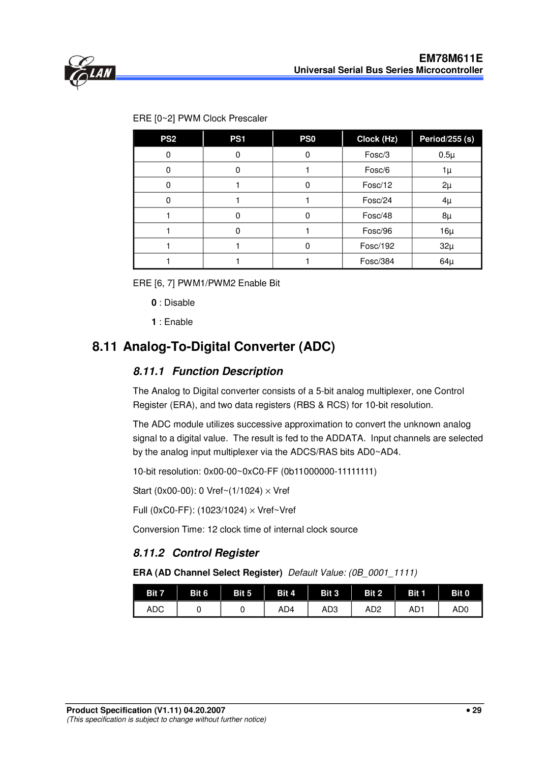
ERE [0~2] PWM Clock Prescaler
PS2 |
| PS1 |
| PS0 | Clock (Hz) |
| Period/255 (s) |
|
|
|
|
|
|
|
|
0 |
| 0 |
| 0 | Fosc/3 |
| 0.5µ |
|
|
|
|
|
|
|
|
0 |
| 0 |
| 1 | Fosc/6 |
| 1µ |
|
|
|
|
|
|
|
|
0 |
| 1 |
| 0 | Fosc/12 |
| 2µ |
|
|
|
|
|
|
|
|
0 |
| 1 |
| 1 | Fosc/24 |
| 4µ |
|
|
|
|
|
|
|
|
1 |
| 0 |
| 0 | Fosc/48 |
| 8µ |
|
|
|
|
|
|
|
|
1 |
| 0 |
| 1 | Fosc/96 |
| 16µ |
|
|
|
|
|
|
|
|
1 |
| 1 |
| 0 | Fosc/192 |
| 32µ |
|
|
|
|
|
|
|
|
1 |
| 1 |
| 1 | Fosc/384 |
| 64µ |
|
|
|
|
|
|
|
|
ERE [6, 7] PWM1/PWM2 Enable Bit
0 : Disable
1 : Enable
8.11 Analog-To-Digital Converter (ADC)
8.11.1 Function Description
The Analog to Digital converter consists of a
The ADC module utilizes successive approximation to convert the unknown analog signal to a digital value. The result is fed to the ADDATA. Input channels are selected by the analog input multiplexer via the ADCS/RAS bits AD0~AD4.
Start
Full
Conversion Time: 12 clock time of internal clock source
8.11.2 Control Register
ERA (AD Channel Select Register) Default Value: (0B_0001_1111)
Bit 7 | Bit 6 | Bit 5 | Bit 4 | Bit 3 | Bit 2 | Bit 1 | Bit 0 |
|
|
|
|
|
|
|
|
ADC
0
0
AD4
AD3
AD2
AD1
AD0
Product Specification (V1.11) 04.20.2007 | • 29 |
(This specification is subject to change without further notice)