EM78M611E
Universal Serial Bus Series Microcontroller
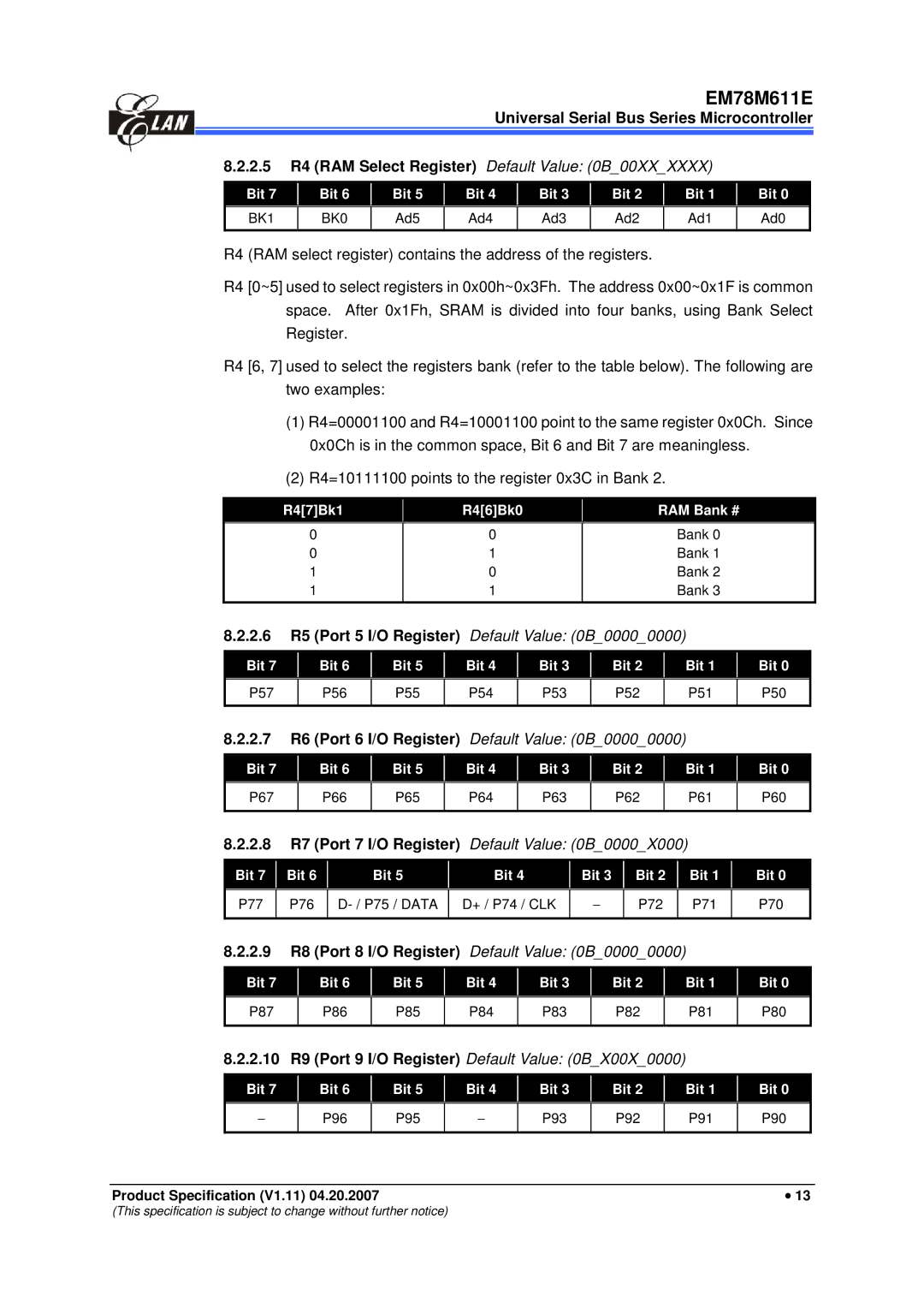
8.2.2.5R4 (RAM Select Register) Default Value: (0B_00XX_XXXX)
Bit 7 |
| Bit 6 |
| Bit 5 |
| Bit 4 |
| Bit 3 |
| Bit 2 |
| Bit 1 |
| Bit 0 |
BK1 |
| BK0 |
| Ad5 |
| Ad4 |
| Ad3 |
| Ad2 |
| Ad1 |
| Ad0 |
|
|
|
|
|
|
|
|
|
|
|
|
|
|
|
R4 (RAM select register) contains the address of the registers.
R4 [0~5] used to select registers in 0x00h~0x3Fh. The address 0x00~0x1F is common space. After 0x1Fh, SRAM is divided into four banks, using Bank Select Register.
R4 [6, 7] used to select the registers bank (refer to the table below). The following are two examples:
(1)R4=00001100 and R4=10001100 point to the same register 0x0Ch. Since 0x0Ch is in the common space, Bit 6 and Bit 7 are meaningless.
(2)R4=10111100 points to the register 0x3C in Bank 2.
R4[7]Bk1 | R4[6]Bk0 | RAM Bank # |
|
|
|
0
0
1
1
0
1
0
1
Bank 0
Bank 1
Bank 2
Bank 3
8.2.2.6 | R5 (Port 5 I/O Register) | Default Value: (0B_0000_0000) |
| ||||||
|
|
|
|
|
|
|
|
|
|
Bit 7 |
| Bit 6 | Bit 5 |
| Bit 4 | Bit 3 | Bit 2 | Bit 1 | Bit 0 |
|
|
|
|
|
|
|
|
|
|
P57 |
| P56 | P55 |
| P54 | P53 | P52 | P51 | P50 |
|
|
|
|
|
|
|
|
|
|
8.2.2.7 | R6 (Port 6 I/O Register) | Default Value: (0B_0000_0000) |
| ||||||
|
|
|
|
|
|
|
|
|
|
Bit 7 |
| Bit 6 | Bit 5 |
| Bit 4 | Bit 3 | Bit 2 | Bit 1 | Bit 0 |
|
|
|
|
|
|
|
|
|
|
P67
P66
P65
P64
P63
P62
P61
P60
8.2.2.8 |
|
| R7 | (Port 7 I/O Register) | Default Value: (0B_0000_X000) |
|
|
|
| |||||||||||||||||||||||||||
|
|
|
|
|
|
|
|
|
|
|
|
|
|
|
|
|
|
|
|
|
|
|
|
|
|
|
|
|
|
|
|
|
|
|
| |
| Bit 7 |
|
| Bit 6 |
|
|
|
| Bit 5 |
|
|
| Bit 4 |
|
| Bit 3 |
|
| Bit 2 |
|
| Bit 1 |
|
| Bit 0 |
| ||||||||||
|
|
|
|
|
|
|
|
|
|
|
|
|
|
|
|
|
|
|
|
|
|
|
|
|
|
|
|
|
|
|
|
|
|
|
|
|
| P77 |
|
| P76 |
|
|
|
|
| D+ / P74 / CLK |
|
|
| − |
|
| P72 |
|
| P71 |
|
| P70 |
| ||||||||||||
|
|
|
|
|
|
|
|
|
|
|
|
|
|
|
|
|
|
|
|
|
|
|
|
|
|
|
|
|
|
|
|
| ||||
8.2.2.9 |
|
| R8 | (Port 8 I/O Register) | Default Value: (0B_0000_0000) |
|
|
|
| |||||||||||||||||||||||||||
|
|
|
|
|
|
|
|
|
|
|
|
|
|
|
|
|
|
|
|
|
|
|
|
|
| |||||||||||
| Bit 7 |
|
|
|
| Bit 6 |
| Bit 5 |
|
| Bit 4 |
|
| Bit 3 |
|
|
| Bit 2 |
|
| Bit 1 |
|
| Bit 0 |
| |||||||||||
|
|
|
|
|
|
|
|
|
|
|
|
|
|
|
|
|
|
|
|
|
|
|
|
|
|
|
|
|
|
|
|
|
|
|
|
|
| P87 |
|
|
|
| P86 |
| P85 |
|
| P84 |
|
| P83 |
|
|
| P82 |
|
| P81 |
|
| P80 |
| |||||||||||
|
|
|
|
|
|
|
|
|
|
|
|
|
|
|
|
|
|
|
|
| ||||||||||||||||
8.2.2.10 | R9 | (Port 9 I/O Register) Default Value: (0B_X00X_0000) |
|
|
|
|
| |||||||||||||||||||||||||||||
|
|
|
|
|
|
|
|
|
|
|
|
|
|
|
|
|
|
| ||||||||||||||||||
| Bit 7 |
|
|
|
| Bit 6 |
| Bit 5 |
|
| Bit 4 |
|
| Bit 3 |
|
|
| Bit 2 |
|
| Bit 1 |
|
| Bit 0 |
| |||||||||||
|
|
|
|
|
|
|
|
|
|
|
|
|
|
|
|
|
|
|
|
|
|
|
|
|
|
|
|
|
|
|
|
|
|
|
|
|
| − |
|
|
|
| P96 |
| P95 |
|
| − |
|
| P93 |
|
|
| P92 |
|
| P91 |
|
| P90 |
| |||||||||||
|
|
|
|
|
|
|
|
|
|
|
|
|
|
|
|
|
|
|
|
|
|
|
|
|
|
|
|
|
|
|
|
|
|
|
| |
|
|
|
|
|
|
|
|
|
|
|
|
|
|
|
|
|
|
|
|
|
|
|
|
|
|
|
|
|
|
|
|
|
|
|
|
|
Product Specification (V1.11) 04.20.2007 |
|
|
|
|
|
|
|
|
|
|
|
|
|
|
|
|
|
| • 13 | |||||||||||||||||
(This specification is subject to change without further notice)