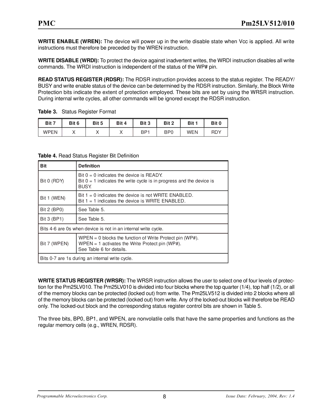
Pm25LV512, Pm25LV010 specifications
PMC-Sierra is renowned for its high-performance semiconductor solutions, and the PM25LV010 and PM25LV512 are standout products in their lineup of serial NOR flash memory devices. These memory chips are specifically designed for a range of applications that include networking, storage, and consumer electronics, providing reliable performance and efficient data storage.The PM25LV010 offers 1 megabit of storage capacity, while the PM25LV512 provides 512 kilobits. Both devices feature a simple serial interface that allows for quick and easy connections to various microcontrollers and digital signal processors. This makes them particularly attractive for systems that require fast access to stored data and simplified design architecture.
One of the primary features of the PM25LV010 and PM25LV512 is their high-speed read capability. With access times as low as 45 nanoseconds, these chips enable rapid data retrieval, ensuring that systems can operate effectively without bottlenecks caused by slow memory access. This is particularly crucial in applications where real-time data processing is essential, such as in communications systems or digital signal processing.
In terms of technology, both devices utilize advanced CMOS manufacturing processes that enhance their reliability and performance. They offer flexibility in programming and erasing, with full chip erase functionality and the ability to program data on a page basis. This allows for efficient updates to the stored information without the need to erase large sections of memory.
Power efficiency is another critical aspect of the PM25LV010 and PM25LV512. These devices consume very little power during both active and standby modes, making them suitable for battery-operated devices and energy-sensitive applications. Their low power consumption ensures extended operation time, which is a significant advantage in portable consumer electronics.
Additionally, both chips are designed with robust security features that aid in protecting sensitive data from unauthorized access. They support a variety of locking and protection mechanisms, ensuring that critical information remains confidential.
In summary, the PMC-Sierra PM25LV010 and PM25LV512 serial NOR flash memory devices merge high-speed performance, low power consumption, and advanced security, making them excellent choices for diverse applications in the modern digital landscape. Their design and technology cater to the growing demand for efficient, reliable, and secure memory solutions in today's rapidly evolving electronic ecosystems.

