ARM720T_LH79520 – Sharp LH79520 SoC with ARM720T
•cs0 (Bank 0) – 4000_0000h to 43FF_FFFFh
•cs1 (Bank 1) – 4400_0000h to 47FF_FFFFh
•cs2 (Bank 2) – 4800_0000h to 4BFF_FFFFh
•cs3 (Bank 3) – 4C00_0000h to 4FFF_FFFFh
•cs4 (Bank 4) – 5000_0000h to 53FF_FFFFh
•cs5 (Bank 5) – 5400_0000h to 57FF_FFFFh
•cs6 (Bank 6) – 5800_0000h to 5BFF_FFFFh
The bank select signals arrive at the processor's wrapper component in the FPGA on the PER_CS bus.
The block of addresses between 5C00_0000h and 5FFF_FFFFh are RESERVED. Software should not access this range of addresses as doing so will not generate a data abort.
In addition, the lowest bank of external memory – Bank 0 – is mirrored to the lowest page (512MBytes) of the processor's address space, in the range 0000_0000h to 1FFF_FFFFh. This occurs by default after a reset is issued and ensures that exception vectors are correctly placed at addresses 0000_0000h to 0000_001Ch.
Of the seven banks of external memory available, six
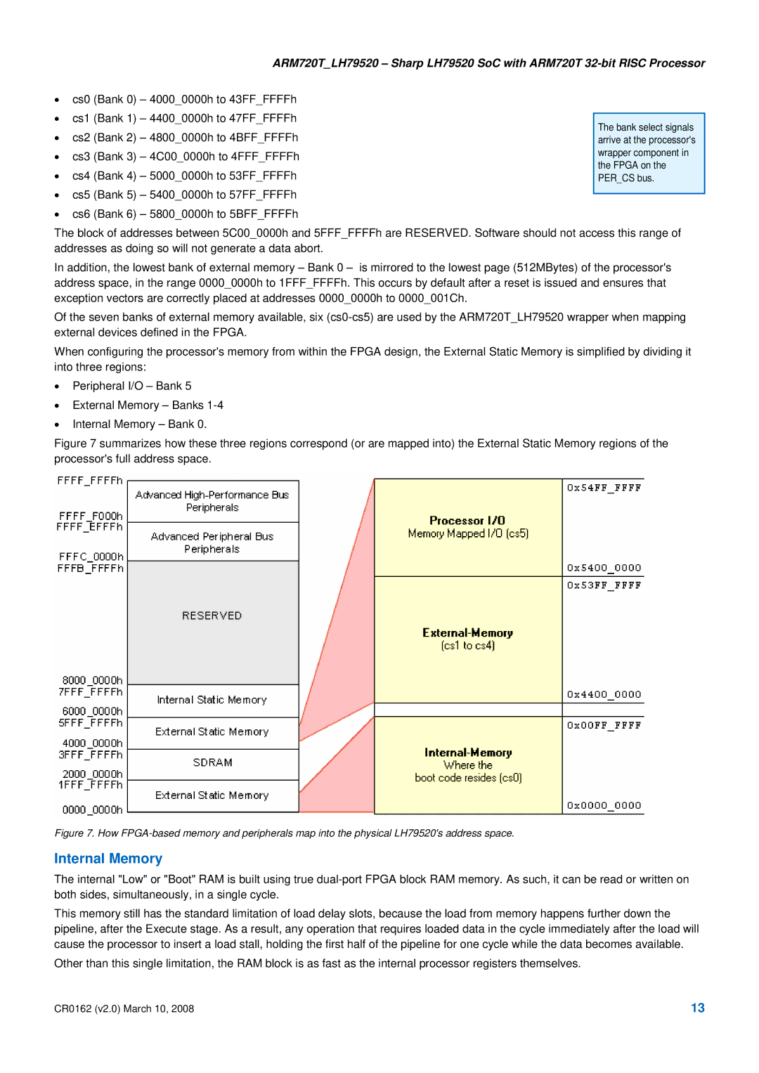
When configuring the processor's memory from within the FPGA design, the External Static Memory is simplified by dividing it into three regions:
•Peripheral I/O – Bank 5
•External Memory – Banks
•Internal Memory – Bank 0.
Figure 7 summarizes how these three regions correspond (or are mapped into) the External Static Memory regions of the processor's full address space.
Figure 7. How FPGA-based memory and peripherals map into the physical LH79520's address space.
Internal Memory
The internal "Low" or "Boot" RAM is built using true
This memory still has the standard limitation of load delay slots, because the load from memory happens further down the pipeline, after the Execute stage. As a result, any operation that requires loaded data in the cycle immediately after the load will cause the processor to insert a load stall, holding the first half of the pipeline for one cycle while the data becomes available.
Other than this single limitation, the RAM block is as fast as the internal processor registers themselves.
CR0162 (v2.0) March 10, 2008 | 13 |