ARM720T_LH79520 – Sharp LH79520 SoC with ARM720T
Placing an ARM720T_LH79520 in an FPGA design
How the ARM720T_LH79520 is placed and wired within an FPGA design depends on the method used to build that design. The main
Design using a Schematic only
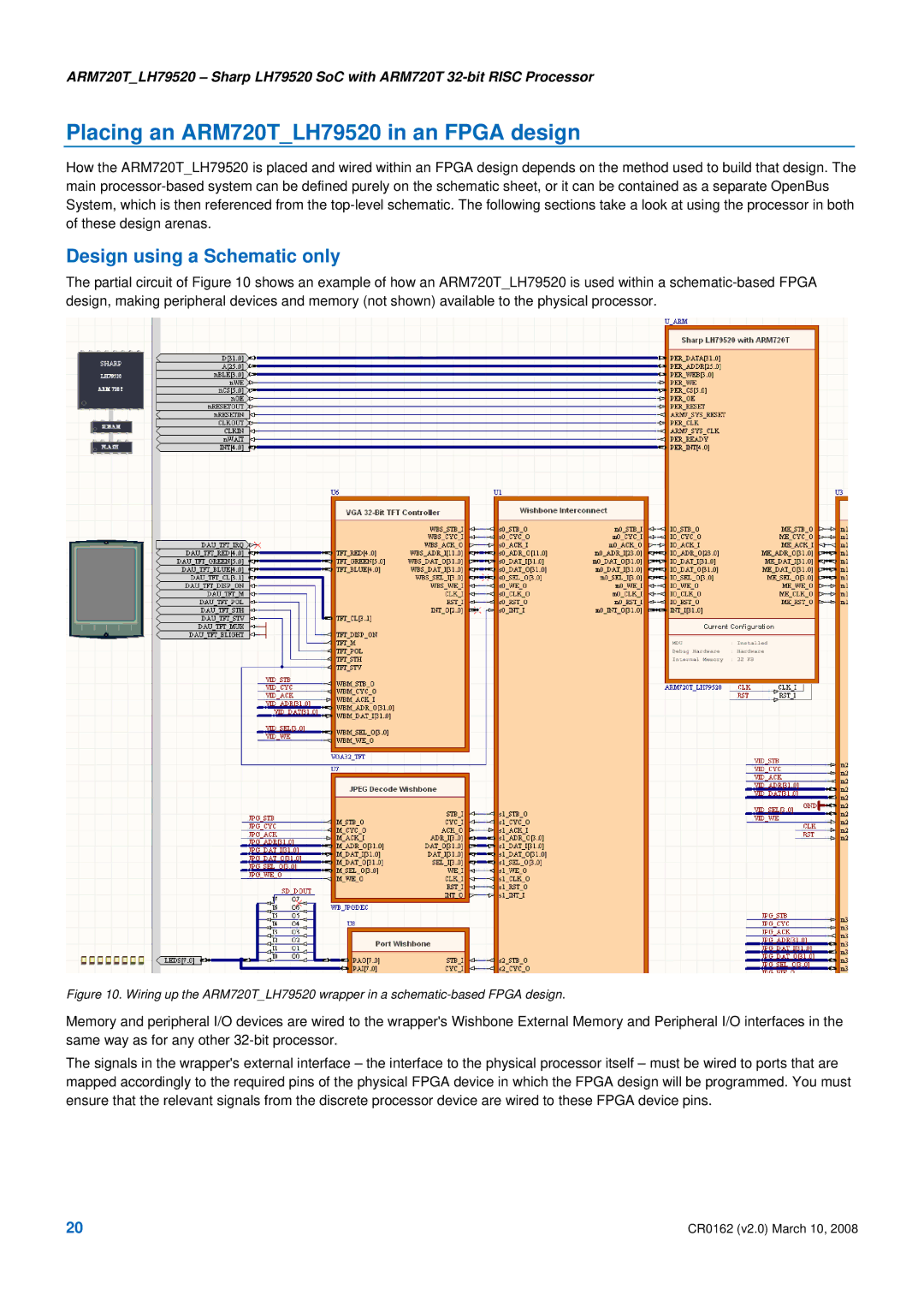
The partial circuit of Figure 10 shows an example of how an ARM720T_LH79520 is used within a
Figure 10. Wiring up the ARM720T_LH79520 wrapper in a schematic-based FPGA design.
Memory and peripheral I/O devices are wired to the wrapper's Wishbone External Memory and Peripheral I/O interfaces in the same way as for any other
The signals in the wrapper's external interface – the interface to the physical processor itself – must be wired to ports that are mapped accordingly to the required pins of the physical FPGA device in which the FPGA design will be programmed. You must ensure that the relevant signals from the discrete processor device are wired to these FPGA device pins.
20 | CR0162 (v2.0) March 10, 2008 |