ARM720T_LH79520 – Sharp LH79520 SoC with ARM720T
Reading from a Slave Wishbone Memory Device
Data is read by the host processor (Wishbone Master) from a
•The host presents an address on its ME_ADR_O output for the address in memory that it wishes to read. It then negates its ME_WE_O output to specify a Read cycle
•The host defines where it expects the data to appear on its ME_DAT_I line using its ME_SEL_O signal
•The slave device receives the address at its ADR_I input and prepares to transmit the data from the selected memory location
•The host asserts its ME_STB_O and ME_CYC_O outputs, indicating that the transfer is to begin. The slave device, monitoring its STB_I and CYC_I inputs, reacts to this assertion by presenting the valid data from the requested memory location at its DAT_O output and asserting its ACK_O signal – to indicate to the host that valid data is present
•The host, monitoring its ME_ACK_I input, responds by latching the data appearing at its ME_DAT_I input and negating the ME_STB_O and ME_CYC_O signals. At the same time, the slave device negates the ACK_O signal and the data transfer cycle is naturally terminated.
Wishbone Timing
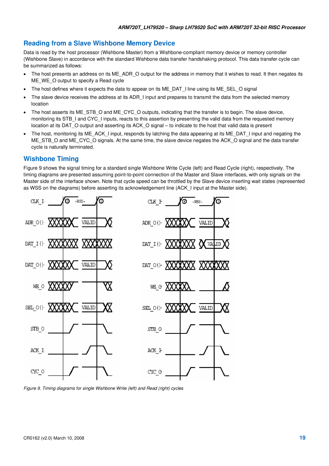
Figure 9 shows the signal timing for a standard single Wishbone Write Cycle (left) and Read Cycle (right), respectively. The timing diagrams are presented assuming point-to-point connection of the Master and Slave interfaces, with only signals on the Master side of the interface shown. Note that cycle speed can be throttled by the Slave device inserting wait states (represented as WSS on the diagrams) before asserting its acknowledgement line (ACK_I input at the Master side).
Figure 9. Timing diagrams for single Wishbone Write (left) and Read (right) cycles
CR0162 (v2.0) March 10, 2008 | 19 |