ARM720T_LH79520 – Sharp LH79520 SoC with ARM720T
Pin Description
The following pin description is for the processor when used on the schematic. In an OpenBus System, although the same signals are present, the abstract nature of the system hides the
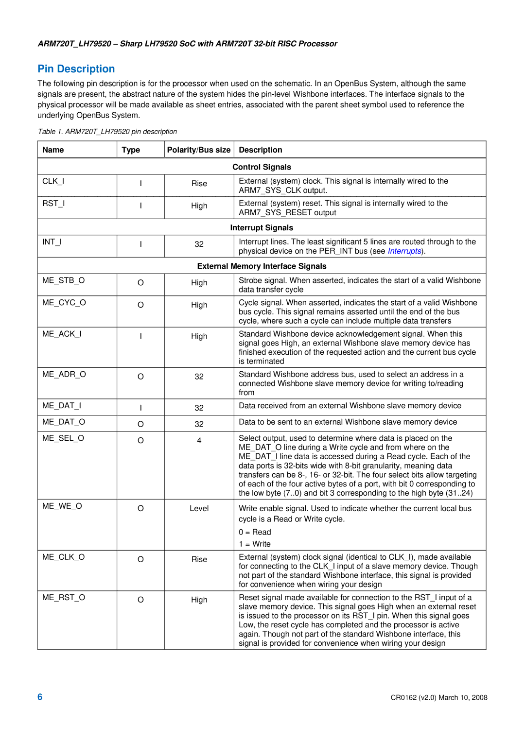
Table 1. ARM720T_LH79520 pin description
Name | Type | Polarity/Bus size |
| Description |
|
|
|
|
|
|
|
| Control Signals | |
|
|
|
|
|
CLK_I | I | Rise |
| External (system) clock. This signal is internally wired to the |
|
|
|
| ARM7_SYS_CLK output. |
RST_I | I | High |
| External (system) reset. This signal is internally wired to the |
|
|
|
| ARM7_SYS_RESET output |
|
| Interrupt Signals | ||
|
|
|
|
|
INT_I | I | 32 |
| Interrupt lines. The least significant 5 lines are routed through to the |
|
|
|
| physical device on the PER_INT bus (see Interrupts). |
|
| External Memory Interface Signals | ||
|
|
|
|
|
ME_STB_O | O | High |
| Strobe signal. When asserted, indicates the start of a valid Wishbone |
|
|
|
| data transfer cycle |
ME_CYC_O | O | High |
| Cycle signal. When asserted, indicates the start of a valid Wishbone |
|
|
|
| bus cycle. This signal remains asserted until the end of the bus |
|
|
|
| cycle, where such a cycle can include multiple data transfers |
ME_ACK_I | I | High |
| Standard Wishbone device acknowledgement signal. When this |
|
|
|
| signal goes High, an external Wishbone slave memory device has |
|
|
|
| finished execution of the requested action and the current bus cycle |
|
|
|
| is terminated |
ME_ADR_O | O | 32 |
| Standard Wishbone address bus, used to select an address in a |
|
|
|
| connected Wishbone slave memory device for writing to/reading |
|
|
|
| from |
ME_DAT_I | I | 32 |
| Data received from an external Wishbone slave memory device |
|
|
|
|
|
ME_DAT_O | O | 32 |
| Data to be sent to an external Wishbone slave memory device |
|
|
|
|
|
ME_SEL_O | O | 4 |
| Select output, used to determine where data is placed on the |
|
|
|
| ME_DAT_O line during a Write cycle and from where on the |
|
|
|
| ME_DAT_I line data is accessed during a Read cycle. Each of the |
|
|
|
| data ports is |
|
|
|
| transfers can be |
|
|
|
| of each of the four active bytes of a port, with bit 0 corresponding to |
|
|
|
| the low byte (7..0) and bit 3 corresponding to the high byte (31..24) |
ME_WE_O | O | Level |
| Write enable signal. Used to indicate whether the current local bus |
|
|
|
| cycle is a Read or Write cycle. |
|
|
|
| 0 = Read |
|
|
|
| 1 = Write |
|
|
|
|
|
ME_CLK_O | O | Rise |
| External (system) clock signal (identical to CLK_I), made available |
|
|
|
| for connecting to the CLK_I input of a slave memory device. Though |
|
|
|
| not part of the standard Wishbone interface, this signal is provided |
|
|
|
| for convenience when wiring your design |
ME_RST_O | O | High |
| Reset signal made available for connection to the RST_I input of a |
|
|
|
| slave memory device. This signal goes High when an external reset |
|
|
|
| is issued to the processor on its RST_I pin. When this signal goes |
|
|
|
| Low, the reset cycle has completed and the processor is active |
|
|
|
| again. Though not part of the standard Wishbone interface, this |
|
|
|
| signal is provided for convenience when wiring your design |
6 | CR0162 (v2.0) March 10, 2008 |